Service hotline
+86 0755-83044319
release time:2024-01-31Author source:SlkorBrowse:16336
MOS field-effect transistor (FET) is a kind of semiconductor device which works on the principle of field effect. Compared with common bipolar transistors, FET has the characteristics of high input impedance, low noise, large dynamic range, low power consumption and easy integration, and has been widely used.
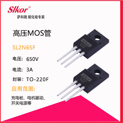
SLKOR MOSFET
There are many kinds of field effect transistors, which are mainly divided into junction field effect transistors and insulated gate field effect transistors. They all have N-channel and P-channel.
Gate field effect transistor is also called metal oxide semiconductor field effect transistor (MOSFET), which is divided into depletion type MOS transistor and enhancement type MOS transistor.
Field effect transistors can be divided into single-gate transistors and double-gate transistors. Double-gate FET has two independent gates G1 and G2, which are structurally equivalent to two single-gate FET connected in series, and the change of its output current is controlled by two gate voltages. This feature of double-gate FET will bring great convenience when it is used as high-frequency amplifier, gain-controlled amplifier, mixer and demodulator.
1. Types and structures of mos tubes
MOSFET is a kind of FET (the other is JFET), which can be made into enhancement or depletion type, P-channel or N-channel. However, the theoretical application only needs enhancement type N-channel MOS transistor and enhancement type P-channel MOS transistor, so NMOS or PMOS is usually mentioned. As for why depletion MOS transistors are not used, it is not recommended to find out. As for these two enhancement MOS transistors, NMOS is commonly used. The reason is that the on-resistance is low and it is easy to manufacture. Therefore, in the application of switching power supply and motor drive, NMOS is usually used. In the following introduction, NMOS is also the main bit. There is parasitic capacitance between the three pins of MOS transistor, which is not what we need, but due to the limitation of manufacturing process. The existence of parasitic capacitance makes the design or selection of driving circuit easier, but there is no way to avoid it, which will be described in detail later. It can be seen in the schematic diagram of MOS transistor that there is a parasitic diode between the drain and the source. This diode is very important when driving a reasonable load. Incidentally, the body diode only exists in a single metal oxide semiconductor transistor, which is usually not found in integrated circuit chips.
2. Conduction characteristics of MOSFET
On means that, as a switch, it is equivalent to the switch closing. NMOS features, when Vgs is greater than a certain value, it will turn on, which is suitable for the case where the source is grounded (low-side driving), as long as the gate voltage reaches 4V or 10V. The characteristics of PMOS, when Vgs is less than a certain value, it will turn on, which is suitable for the source connection VCC (high-side drive). However, although PMOS can be easily used as a high-end driver, NMOS is usually used as a high-end driver because of its high resistance, high price and few AC types.3. Metal oxide semiconductor switch tube
3. MOSFET Switch
No matter whether the loss is NMOS or PMOS, there is an on-resistance after conduction, so the current will consume the energy on this resistance, which is called on-loss Choose MOS transistor with low on resistance to reduce on loss. Usually, the on-resistance of low-power MOS tubes is about tens of milliohms, and some of them are turned on and off in a few milliohms. MOS must not be completed instantly. The voltage at both ends of MOS decreases and the current increases. During this period, the loss of MOS transistor is the product of voltage and current, which is called switching loss. Generally, the switching loss is far greater than the conduction loss, and the faster the switching frequency, the greater the loss. The product of instantaneous voltage and current is very large, and the resulting loss is also very large. Shortening the switching time can reduce each conduction time; The loss reduction of switching frequency can reduce the switching times per unit time. Both methods can reduce the switching loss.
4. MOSFET Driving
Compared with bipolar transistors, it is generally believed that MOS transistors don't need current for conduction, but only need GS voltage higher than a certain value. It's easy to do, but we still need speed. In the structure of MOS transistor, we can see that there is parasitic capacitance between GS and GD. Theoretically, the driving of MOS transistor is the charging and discharging of capacitance. Current is needed to charge the capacitor. Because the capacitor can be regarded as a short circuit at the moment of charging, the instantaneous current will be relatively large.
When selecting/designing MOS transistor drivers, the first thing to pay attention to is the instantaneous short-circuit current. The second note is that NMOS commonly used in high-side driving requires that the gate voltage when it is turned on is higher than the source voltage. On the other hand, the source voltage and drain voltage (VCC) of high-side driving MOS transistor are the same, so the gate voltage is 4V or 10V higher than VCC. Assume that in the same system, in order to obtain a voltage larger than VCC, a special boost circuit is needed. Many motor drivers are integrated with charge pumps. It should be noted that an appropriate external capacitor should be selected to obtain enough short-circuit current to drive the metal oxide semiconductor transistor. The above mentioned 4V or 10V is the turn-on voltage of common MOS transistors, so there is certainly some margin in the design. In addition, the higher the voltage, the faster the conduction speed and the smaller the conduction resistance. MOS tubes with low conduction voltage are always used in different categories, but in 12V automotive electronic systems, ordinary 4v conduction is enough.
The main parameters of MOS tube are as follows:
1. Gate-source breakdown voltage BVGS-VGS When the gate current IG increases sharply from zero, the gate-source voltage increases, which is called the gate-source breakdown voltage BVGS.
2. Turning-on voltage VT- Turning-on voltage (also called threshold voltage): the starting end between the source S and the drain D forms a conducting channel; -The required gate voltage of standard N-channel MOS transistor is about 3 ~ 6V-.-The VT value of MOS transistor can be reduced to 2 ~ 3V after process improvement.
3. The drain-source breakdown voltage BVDS- Under the condition of VGS=0 (enhancement mode), VDS is called the drain-source breakdown voltage BVDS-ID in the process when ID starts to increase sharply. There are two reasons for the growth:
(1) Avalanche breakdown of depletion layer near the left side of drain.
(2) Drain-source punch-through breakdown-in some MOS, the channel length is short. Increasing VDS from time to time will make the drain depletion layer extend to the source region from time to time, making the channel length zero, that is, drain-source punch-through. After punch-through, most carriers in the source region will be directly absorbed by the electric field in the depletion layer and reach the drain region, resulting in a large ID.4. The characteristic of
4. DC input resistance RGS-that is, the ratio of voltage applied between gate and source to gate current-is sometimes expressed by the gate current flowing through the gate RGS of metal oxide semiconductor transistor, which easily exceeds 1010.5. Low-frequency transconductance GM-Under the condition that VDS is a fixed value, the ratio of the micro-variable of drain current to the micro-variable of gate-source voltage that causes this change is called transconductance-GM reflects the control ability of gate-source voltage to drain current-it is an important parameter to characterize the amplification ability of MOS transistors-usually in the range of several Ma/V.



Site Map | 萨科微 | 金航标 | Slkor | Kinghelm
RU | FR | DE | IT | ES | PT | JA | KO | AR | TR | TH | MS | VI | MG | FA | ZH-TW | HR | BG | SD| GD | SN | SM | PS | LB | KY | KU | HAW | CO | AM | UZ | TG | SU | ST | ML | KK | NY | ZU | YO | TE | TA | SO| PA| NE | MN | MI | LA | LO | KM | KN
| JW | IG | HMN | HA | EO | CEB | BS | BN | UR | HT | KA | EU | AZ | HY | YI |MK | IS | BE | CY | GA | SW | SV | AF | FA | TR | TH | MT | HU | GL | ET | NL | DA | CS | FI | EL | HI | NO | PL | RO | CA | TL | IW | LV | ID | LT | SR | SQ | SL | UK
Copyright ©2015-2025 Shenzhen Slkor Micro Semicon Co., Ltd