Service hotline
+86 0755-83044319

release time:2024-06-19Author source:SlkorBrowse:17386
On June 16th, ASML, the global leader in lithography machines, announced a remarkable technological advancement. They have not only successfully delivered the world's first High NA EUV (Extreme Ultraviolet) lithography machine to Intel but are also actively developing even more advanced Hyper NA EUV machines. This technology is expected to push semiconductor processes to unprecedented levels down to 0.2nm, equivalent to 2Å (angstroms).
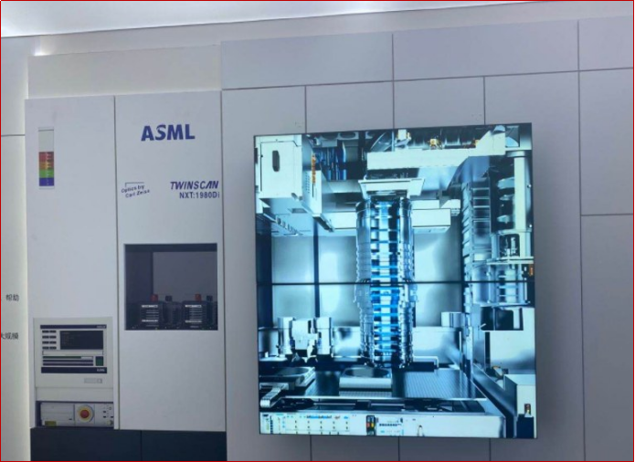
ASML's strategic focus in the field of lithography is clearly delineated with their development of Low NA, High NA, and potential future Hyper NA EUV (Extreme Ultraviolet) lithography machines.
Firstly, the Low NA EUV lithography machines, under the NXE series with a numerical aperture (NA) of 0.33, include models like the 3400B/C, 3600D, and 3800E, with future models expected such as the 4000F, 4200G, and beyond. ASML aims to achieve volume production for 2nm processes by 2025, progressing to 1.4nm by 2027 with the aid of multi-patterning techniques.
Expanding beyond Low NA, ASML introduced the High NA EUV lithography machines, part of the EXE series featuring an NA of 0.55. This series includes models like the 5000, 5200B, with future models anticipated such as the 5400, 5600, and beyond. High NA lithography starts below 2nm processes, with Intel already adopting the 14A 1.4nm process. ASML forecasts achieving volume production for 1nm processes around 2029, potentially scaling down to 0.5nm or 0.7nm by 2033 with multi-patterning.
Looking even further ahead, ASML is researching Hyper NA EUV lithography with an NA potentially reaching 0.75 or higher. The HXE series, expected around 2030, aims to enable processes as advanced as 0.2nm, although the feasibility and specific performance characteristics are still being refined.
It's important to note that these node sizes, such as 0.2nm, do not directly correspond to physical transistor dimensions but rather represent significant advancements in performance and efficiency ratios. For instance, the metal pitch for 0.2nm nodes may range between 16-12nm initially, progressing to 14-10nm.
ASML's strategy involves utilizing a single EUV platform across Low/High/Hyper NA lithography machines, facilitating cost-effective development, manufacturing, and deployment. This approach ensures smooth transitions and upgrades between technologies.
However, as technological limits approach, challenges intensify. High NA lithography machines already command prices around €350 million each, and costs are expected to rise further for Hyper NA machines. Moreover, the physical limits of lithography technology are becoming increasingly apparent as dimensions shrink.
Despite these challenges, ASML and the semiconductor industry continue to pursue breakthroughs and innovations to address future opportunities and challenges in microelectronics.
Site Map | 萨科微 | 金航标 | Slkor | Kinghelm
RU | FR | DE | IT | ES | PT | JA | KO | AR | TR | TH | MS | VI | MG | FA | ZH-TW | HR | BG | SD| GD | SN | SM | PS | LB | KY | KU | HAW | CO | AM | UZ | TG | SU | ST | ML | KK | NY | ZU | YO | TE | TA | SO| PA| NE | MN | MI | LA | LO | KM | KN
| JW | IG | HMN | HA | EO | CEB | BS | BN | UR | HT | KA | EU | AZ | HY | YI |MK | IS | BE | CY | GA | SW | SV | AF | FA | TR | TH | MT | HU | GL | ET | NL | DA | CS | FI | EL | HI | NO | PL | RO | CA | TL | IW | LV | ID | LT | SR | SQ | SL | UK
Copyright ©2015-2025 Shenzhen Slkor Micro Semicon Co., Ltd
