Service hotline
+86 0755-83044319
release time:2022-03-17Author source:SlkorBrowse:11810
Abstract: With the continuous breakthrough of silicon-based gallium nitride epitaxial technology, the localization of its special silicon substrate materials has become increasingly prominent. This paper analyzes the problems of dense and split edge slip lines after domestic wafer epitaxy, and puts forward the parameters and technical indexes of silicon wafer edge control and mechanical strength control, which points out a certain direction for the development of high-quality silicon substrate to meet the demand of power device-level GaN epitaxy.
Preparation method: CZ (Czochralski method);
Conductive type: P type;
Doping agent: boron doping;
Orientation: < 111 >;
Diameter: 150.0± 0.3 mm;
Thickness: 1 000± 15 μm;
Single-sided polishing, no cleaning.
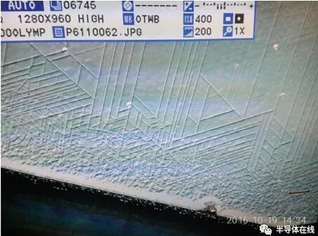
Fig. 1 Microscopic photograph of edge slip line
At the same time, three domestic wafers and three imported wafers were used for epitaxial growth in the same furnace. During the cooling process, all three domestic wafers were split into two halves, and all three imported wafers were intact. The curve of curvature change in the growth process is shown in Figure 2.
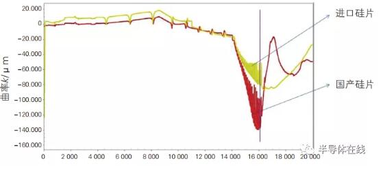
T/s
Fig. 2 Variation diagram of epitaxial growth curvature
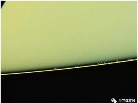
Fig. 3 Chamfer edge of grinding wheel with grain size of 11.0μ m.
When CZ silicon wafer with thickness of 1 000μm is used for epitaxial growth of gallium nitride, it shows that the internal stress of the silicon wafer itself is large in the thermal process, and the mechanical strength can not meet the requirements. The stress of silicon wafer comes from the internal stress generated during the growth of single crystal and the stress introduced during processing. The mechanical strength of silicon wafer mainly depends on the internal defects of silicon single crystal and the mechanical damage caused by processing. In order to improve the mechanical strength of silicon wafer, we should start from three aspects: crystal performance of silicon single crystal, damage control during processing, surface quality and geometric parameters control.
2.2.1 quality control of silicon single crystal
The internal defects and oxygen content of silicon single crystal have an important influence on the mechanical properties of silicon wafers. In addition, the doping, thickness and crystal orientation of silicon wafers are also important parameters that affect the mechanical strength of silicon wafers. We analyzed and tested domestic silicon wafers and imported silicon wafers respectively, and the results are shown in Table 1. The test results show that both domestic silicon wafers and imported silicon wafers adopt 1 000 μm thick P<111 > heavily doped boron substrate, the < 111 > crystal orientation is mainly to match the hexagonal wurtzite structure of gallium nitride and reduce lattice mismatch, and the heavily doped boron is to improve the mechanical strength of silicon wafers. The doping concentration of imported silicon wafers is one order of magnitude higher than that of domestic silicon wafers, and the resistivity reaches 0.003 6 Ω· Cm, this is a significant difference. There is no difference in oxygen and carbon concentration between domestic silicon wafers and imported silicon wafers, both of which are normal oxygen and carbon content values. However, there are fewer domestic silicon wafers with bulk defects, which shows that there is no difficulty in the preparation of basic single crystals, and the main thing is to control the resistivity of silicon wafers to be consistent with that of imported wafers.
In addition, the stress of the silicon single crystal mainly comes from the growth stress and the stress generated during the cooling process after the growth of the single crystal. At present, the growth technology of the 15.24 cm silicon single crystal is relatively mature, and the key lies in controlling the appropriate growth rate and avoiding the formation of local stress and internal stress due to the rapid cooling of the crystal. Under the same process conditions, the greater the stress of silicon single crystal, the greater the warpage of the cut silicon wafer. The smaller the stress of single crystal silicon, the smaller the warpage of the cut silicon wafer. By monitoring the slice warpage under the same process conditions, the growth process of silicon single crystal is optimized. Generally, the warpage of high-quality single crystal after cutting is not more than 15 μm m.
Table 1 Comparison of crystal parameters between domestic silicon wafers and imported silicon wafe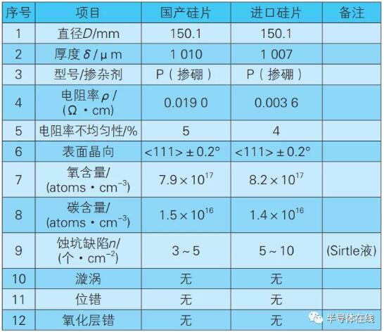
The damage produced in the machining process is mainly the surface damage and edge damage produced in the cutting and grinding process, which are the main factors affecting the strength of silicon wafers. Sumino et al. have studied the tensile properties of dislocation-free silicon single crystal, and found that the surface damage has great influence on the mechanical strength of single crystal, and the yield stress of silicon single crystal with surface damage is obviously lower. Other studies on flexural strength also show that [5], the less the surface damage, the higher the flexural strength. Slicing is the first process that causes the surface damage of the silicon wafer, and it is also the most serious process. Therefore, optimizing the cutting process conditions is particularly important to reduce the surface damage. Optimizing the multi-wire cutting process, adjusting the mortar flow rate and cutting temperature, and minimizing the warpage and curvature of the cut silicon wafer can effectively improve the subsequent bending strength of the silicon wafer. The damage caused by grinding with alumina powder with a nominal particle size of 8 μm can be divided into two parts: 1) The severe damage area consisting of dislocations, cracks and broken grains is located in the range of about 10 μm from the surface of the silicon wafer; 2) The high stress area is located in the range of (10 ~ 25) μ m from the surface of the silicon wafer. Therefore, when we use alkali etching to remove 8 ~ 10μ m, only the broken layer on the surface is partially removed, and the mechanical strength of silicon wafer is only improved compared with that of grinding plate. Due to alkali corrosion, the back surface roughness of domestic chips is as high as 0.6 μm m. By comparing the test results of back surface roughness, the surface roughness of imported chips is only 0.2 μm, which is equivalent to 1/3 of that of domestic chips. Therefore, after grinding, acid etching process should be adopted to remove 25 ~ 30μ m on one side, which can effectively remove the damaged surface layer and improve the mechanical strength. In addition, if necessary, double-sided polishing sheets can be used to greatly improve the mechanical strength of silicon wafers.
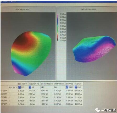
Fig. 5 Test results of geometric parameters of domestic silicon wafers
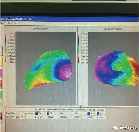
Fig. 6 Test results of geometric parameters of imported silicon wafers
According to the above test and analysis, we have formulated the processing control standard of silicon substrate for gallium nitride. See Table 2. According to the requirements of control parameters, we adjusted the processing conditions, and the epitaxial quality of the 15.24 cm P heavily doped silicon single-sided polishing wafer was the same as that of foreign substrates.
4 Conclusion
In order to solve the problem of slip lines and cracks after silicon-based gallium nitride epitaxy for power devices, we must improve the edge quality and mechanical strength of silicon wafers. This requires us to organically combine the surface control technology of 15.24 cm silicon polishing wafer for silicon epitaxy, the geometric parameter control technology of MEMS silicon wafer and the edge control technology of 20.32~30.48 cm IC silicon wafer in the traditional industry to form a special technical standard for gallium nitride silicon substrate, so as to meet the development requirements of subsequent industrialization.
Table 2 Specification Requirements of Silicon Substrate for GaN Epitaxy
Disclaimer: This article is reproduced from "GaN World". This article only represents the author's personal views, not the views of Sacco Micro and the industry. It is only for reprinting and sharing to support the protection of intellectual property rights. Please indicate the original source and author when reprinting. If there is any infringement, please contact us to delete it.
Company Tel: +86-0755-83044319
Fax/fax:+86-0755-83975897
Email: 1615456225@qq.com
QQ: 3518641314 Manager Li
QQ: 332496225 Manager Qiu
Address: Room 809, Block C, Zhantao Technology Building, No.1079 Minzhi Avenue, Longhua New District, Shenzhen



Site Map | 萨科微 | 金航标 | Slkor | Kinghelm
RU | FR | DE | IT | ES | PT | JA | KO | AR | TR | TH | MS | VI | MG | FA | ZH-TW | HR | BG | SD| GD | SN | SM | PS | LB | KY | KU | HAW | CO | AM | UZ | TG | SU | ST | ML | KK | NY | ZU | YO | TE | TA | SO| PA| NE | MN | MI | LA | LO | KM | KN
| JW | IG | HMN | HA | EO | CEB | BS | BN | UR | HT | KA | EU | AZ | HY | YI |MK | IS | BE | CY | GA | SW | SV | AF | FA | TR | TH | MT | HU | GL | ET | NL | DA | CS | FI | EL | HI | NO | PL | RO | CA | TL | IW | LV | ID | LT | SR | SQ | SL | UK
Copyright ©2015-2025 Shenzhen Slkor Micro Semicon Co., Ltd