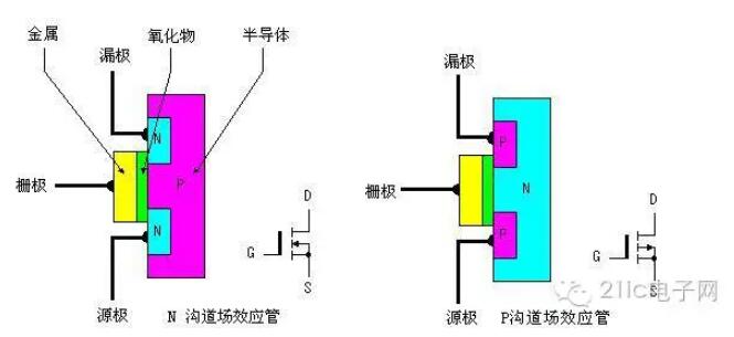
The original meaning of MOSFET is: MOS(Metal Oxide Semiconductor), FET(Field Effect Transistor), that is, the field effect transistor that controls the semiconductor (S) by the effect of electric field with the gate of the metal layer (M) through the oxide layer (O).Structure of power MOSFET
The internal structure and electrical symbol of power MOSFET are shown in the figure. It can be divided into NPN type and PNP type. Type NPN is usually called n-channel type, and type PNP is usually called p-channel type. As can be seen from fig. 1, the source and drain of the N-channel FET are connected to the N-type semiconductor, and the source and drain of the P-channel FET are connected to the P-type semiconductor. We know that the general triode controls the output current by the input current. However, for FET, its output current is controlled by the input voltage (or field voltage). It can be considered that the input current is very small or there is no input current, which makes the device have a high input impedance, and this is why we call it FET.
Working principle of power MOSFET
Cut-off: positive power supply is applied between drain and source, and the voltage between gate and source is zero. The PN junction J1 formed between the P-base region and the N-drift region is reversed, and no current flows between the drain and the source.
Conductivity: A positive voltage UGS is applied between the gate and the source. The gate is insulated, so no gate current will flow. However, the positive voltage of the gate will push away the holes in the P region below it, and attract minority carriers and electrons in the P region to the surface of the P region below the gate.When UGS is greater than UT (turn-on voltage or threshold voltage), the electron concentration on the surface of the P-region under the gate will exceed the hole concentration, which will invert the P-type semiconductor into N-type and become an inversion layer. The inversion layer will form an N-channel to make the PN junction J1 disappear, and the drain and source will be conductive.Basic characteristics of power MOSFET
Static characteristics:
Its transfer characteristics and output characteristics are shown in Figure 2.
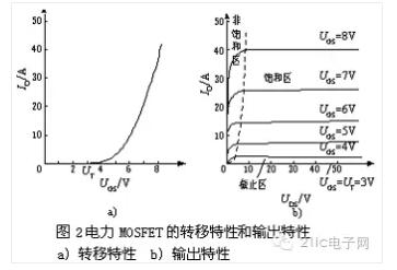
The relationship between drain current ID and gate-source voltage UGS is called the transfer characteristic of MOSFET. When ID is large, the relationship between ID and UGS is approximately linear, and the slope of the curve is defined as transconductance Gfs.
V-A characteristics (output characteristics) of the drain of MOSFET: cut-off region (corresponding to the cut-off region of GTR); Saturation region (corresponding to the amplification region of GTR); Unsaturated region (corresponding to the saturated region of GTR). The power MOSFET works in the switching state, that is, it switches back and forth between the cutoff region and the unsaturated region. There is a parasitic diode between the drain and source of power MOSFET, and the device turns on when a reverse voltage is applied between the drain and source. The on-state resistance of power MOSFET has a positive temperature coefficient, which is beneficial to current sharing when the devices are connected in parallel.
Dynamic characteristics:
The test circuit and switching process waveforms are shown in Figure 3.
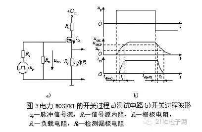 Td(on) turn-on delay time-turn-on delay time is the time from when the gate-source voltage rises to 10% of the gate driving voltage to when the leakage current rises to 10% of the specified current.Tr Rise Time-Rise time is the time it takes for the drain current to rise from 10% to 90%. The steady-state value of iD is determined by the drain power supply voltage UE and the drain load resistance. The size of UGSP is related to the steady-state value of iD. After UGS reaches UGSP, it continues to rise under the action of up until it reaches the steady state, but the iD has not changed. Opening time ton-the sum of opening delay time and rising time.Td(off) turn-off delay time-turn-off delay time is the time from when the gate-source voltage drops to 90% of the gate driving voltage to when the leakage current drops to 90% of the specified current. This shows the delay before the current is transmitted to the load.Tf Fall Time-The fall time is the time it takes for the drain current to drop from 90% to 10%.Turn-off time toff-the sum of turn-off delay time and falling time.
Understand several common parameters of MOSFET VDS, that is, the drain-source voltage, is a limiting parameter of MOSFET, which indicates the maximum voltage between the drain and the source of MOSFET. It should be noted that this parameter is related to the junction temperature. Usually, the higher the junction temperature, the maximum value. RDS(on), on-resistance of drain and source, which indicates on-resistance between drain and source when MOSFET is turned on under certain conditions. This parameter is related to MOSFET junction temperature and driving voltage Vgs. Within a certain range, the higher the junction temperature, the greater the Rds; The higher the driving voltage, the smaller the Rds. Q, gate charge, is the charging charge required for the gate voltage to rise from 0V to the termination voltage (such as 15V) under the action of the driving signal. That is, the charge that the MOSFET needs to provide from the off state to the fully on state is a main parameter used to evaluate the driving capability of the MOSFET driving circuit. Id, drain current and drain current are usually described in several different ways. According to the form of working current, there are continuous drain current and Pulsed drain current with a certain pulse width. This parameter is also a limit parameter of MOSFET, but this maximum current value does not mean that the drain current can reach this value during operation. It means that when the shell temperature is at a certain value, if the MOSFET working current is the above-mentioned maximum drain current, the junction temperature will reach the maximum value. So this parameter is also related to device package and ambient temperature. Eoss, output capacity energy, indicates the energy stored in MOSFET by output capacitor Coss. Because the output capacitance Coss of MOSFET has obvious nonlinear characteristics, it changes with the change of Vds voltage. Therefore, if datasheet provides this parameter, it is very helpful to evaluate the switching loss of MOSFET. Not all MOSFET manuals provide this parameter, in fact, most datasheet do not. The current change rate of Body Diode di/dt body diode reflects the reverse recovery characteristics of MOSFET body diode. Because the diode is a bipolar device, it is affected by charge storage. When the diode is reverse biased, the charge stored in the PN junction must be cleared. The above parameters reflect this characteristic. Vg, the maximum driving voltage of gate and source, which is also a limit parameter of MOSFET, indicates the maximum driving voltage that MOSFET can bear. Once the driving voltage exceeds this limit, it will cause permanent damage to the gate oxide layer even in a very short time. Generally speaking, as long as the driving voltage does not exceed the limit, there will be no problem. However, in some special occasions, because of the existence of parasitic parameters, it will have an unexpected impact on Vgs voltage, which needs special attention. SOA, safe working area, each MOSFET will give its safe working area. Different bipolar transistors and power MOSFETs will not show secondary breakdown, so the safe working area is simply defined from the dissipated power when the junction temperature reaches the maximum allowable value. Selection principle of power MOSFET Knowing the significance of MOSFET parameters, how to choose the products that meet your needs according to the manufacturer's product manual? There are four steps to choose the correct MOSFET.1) Channel Selection The first step in choosing the right device for the design is to decide whether to use N-channel or P-channel MOSFET. In typical power applications, when a MOSFET is grounded and the load is connected to the mains voltage, the MOSFET constitutes a low-voltage side switch. In the low-voltage side switch, N-channel MOSFET should be used because of the consideration of the voltage required to turn off or turn on the device. When the MOSFET is connected to the bus and the load is grounded, the high-voltage side switch is used. P-channel MOSFET is usually used in this topology, which is also due to the consideration of voltage driving. 2) Selection of voltage and current The higher the rated voltage, the higher the cost of the device. According to practical experience, the rated voltage should be greater than the mains voltage or bus voltage. Only in this way can sufficient protection be provided so that the MOSFET will not fail. As far as MOSFET selection is concerned, it is necessary to determine the maximum voltage between the drain and the source, that is, the maximum VDS. Other safety factors that design engineers need to consider include voltage transients induced by switching electronic devices, such as motors or transformers. The rated voltage of different applications is also different; Usually, the portable device is 20V, the FPGA power supply is 20~30V, and the 85~220VAC application is 450~600V V. In the continuous conduction mode, the MOSFET is in a steady state, and the current continuously passes through the device. Pulse spike refers to a large amount of surge (or spike current) flowing through the device. Once the maximum current under these conditions is determined, it is only necessary to directly select the device that can withstand this maximum current. 3) Calculation of conduction loss The power loss of MOSFET devices can be calculated by Iload2× According to RDS(ON) calculation, since the on-resistance changes with temperature, the power consumption will also change proportionally. For portable design, it is easier (more common) to use a lower voltage, while for industrial design, a higher voltage can be used. Note that the RDS(ON) resistance will rise slightly with the current. Changes of various electrical parameters of RDS(ON) resistance can be found in the technical data sheet provided by the manufacturer. 4) The heat dissipation of the computing system requires the designer to consider two different situations, namely, the worst case and the real situation. It is recommended to adopt the calculation result for the worst case, because this result provides a larger safety margin and can ensure that the system will not fail. There are some measurement data that need attention in the MOSFET data sheet; Such as the thermal resistance between the semiconductor junction of the packaged device and the environment, and the maximum junction temperature. In fact, switching loss is also a very important index. The instantaneous voltage-current product is quite large, which determines the switching performance of the device to some extent. However, if the system requires high switching performance, the power MOSFET with low gate charge QG can be selected.
Td(on) turn-on delay time-turn-on delay time is the time from when the gate-source voltage rises to 10% of the gate driving voltage to when the leakage current rises to 10% of the specified current.Tr Rise Time-Rise time is the time it takes for the drain current to rise from 10% to 90%. The steady-state value of iD is determined by the drain power supply voltage UE and the drain load resistance. The size of UGSP is related to the steady-state value of iD. After UGS reaches UGSP, it continues to rise under the action of up until it reaches the steady state, but the iD has not changed. Opening time ton-the sum of opening delay time and rising time.Td(off) turn-off delay time-turn-off delay time is the time from when the gate-source voltage drops to 90% of the gate driving voltage to when the leakage current drops to 90% of the specified current. This shows the delay before the current is transmitted to the load.Tf Fall Time-The fall time is the time it takes for the drain current to drop from 90% to 10%.Turn-off time toff-the sum of turn-off delay time and falling time.
Understand several common parameters of MOSFET VDS, that is, the drain-source voltage, is a limiting parameter of MOSFET, which indicates the maximum voltage between the drain and the source of MOSFET. It should be noted that this parameter is related to the junction temperature. Usually, the higher the junction temperature, the maximum value. RDS(on), on-resistance of drain and source, which indicates on-resistance between drain and source when MOSFET is turned on under certain conditions. This parameter is related to MOSFET junction temperature and driving voltage Vgs. Within a certain range, the higher the junction temperature, the greater the Rds; The higher the driving voltage, the smaller the Rds. Q, gate charge, is the charging charge required for the gate voltage to rise from 0V to the termination voltage (such as 15V) under the action of the driving signal. That is, the charge that the MOSFET needs to provide from the off state to the fully on state is a main parameter used to evaluate the driving capability of the MOSFET driving circuit. Id, drain current and drain current are usually described in several different ways. According to the form of working current, there are continuous drain current and Pulsed drain current with a certain pulse width. This parameter is also a limit parameter of MOSFET, but this maximum current value does not mean that the drain current can reach this value during operation. It means that when the shell temperature is at a certain value, if the MOSFET working current is the above-mentioned maximum drain current, the junction temperature will reach the maximum value. So this parameter is also related to device package and ambient temperature. Eoss, output capacity energy, indicates the energy stored in MOSFET by output capacitor Coss. Because the output capacitance Coss of MOSFET has obvious nonlinear characteristics, it changes with the change of Vds voltage. Therefore, if datasheet provides this parameter, it is very helpful to evaluate the switching loss of MOSFET. Not all MOSFET manuals provide this parameter, in fact, most datasheet do not. The current change rate of Body Diode di/dt body diode reflects the reverse recovery characteristics of MOSFET body diode. Because the diode is a bipolar device, it is affected by charge storage. When the diode is reverse biased, the charge stored in the PN junction must be cleared. The above parameters reflect this characteristic. Vg, the maximum driving voltage of gate and source, which is also a limit parameter of MOSFET, indicates the maximum driving voltage that MOSFET can bear. Once the driving voltage exceeds this limit, it will cause permanent damage to the gate oxide layer even in a very short time. Generally speaking, as long as the driving voltage does not exceed the limit, there will be no problem. However, in some special occasions, because of the existence of parasitic parameters, it will have an unexpected impact on Vgs voltage, which needs special attention. SOA, safe working area, each MOSFET will give its safe working area. Different bipolar transistors and power MOSFETs will not show secondary breakdown, so the safe working area is simply defined from the dissipated power when the junction temperature reaches the maximum allowable value. Selection principle of power MOSFET Knowing the significance of MOSFET parameters, how to choose the products that meet your needs according to the manufacturer's product manual? There are four steps to choose the correct MOSFET.1) Channel Selection The first step in choosing the right device for the design is to decide whether to use N-channel or P-channel MOSFET. In typical power applications, when a MOSFET is grounded and the load is connected to the mains voltage, the MOSFET constitutes a low-voltage side switch. In the low-voltage side switch, N-channel MOSFET should be used because of the consideration of the voltage required to turn off or turn on the device. When the MOSFET is connected to the bus and the load is grounded, the high-voltage side switch is used. P-channel MOSFET is usually used in this topology, which is also due to the consideration of voltage driving. 2) Selection of voltage and current The higher the rated voltage, the higher the cost of the device. According to practical experience, the rated voltage should be greater than the mains voltage or bus voltage. Only in this way can sufficient protection be provided so that the MOSFET will not fail. As far as MOSFET selection is concerned, it is necessary to determine the maximum voltage between the drain and the source, that is, the maximum VDS. Other safety factors that design engineers need to consider include voltage transients induced by switching electronic devices, such as motors or transformers. The rated voltage of different applications is also different; Usually, the portable device is 20V, the FPGA power supply is 20~30V, and the 85~220VAC application is 450~600V V. In the continuous conduction mode, the MOSFET is in a steady state, and the current continuously passes through the device. Pulse spike refers to a large amount of surge (or spike current) flowing through the device. Once the maximum current under these conditions is determined, it is only necessary to directly select the device that can withstand this maximum current. 3) Calculation of conduction loss The power loss of MOSFET devices can be calculated by Iload2× According to RDS(ON) calculation, since the on-resistance changes with temperature, the power consumption will also change proportionally. For portable design, it is easier (more common) to use a lower voltage, while for industrial design, a higher voltage can be used. Note that the RDS(ON) resistance will rise slightly with the current. Changes of various electrical parameters of RDS(ON) resistance can be found in the technical data sheet provided by the manufacturer. 4) The heat dissipation of the computing system requires the designer to consider two different situations, namely, the worst case and the real situation. It is recommended to adopt the calculation result for the worst case, because this result provides a larger safety margin and can ensure that the system will not fail. There are some measurement data that need attention in the MOSFET data sheet; Such as the thermal resistance between the semiconductor junction of the packaged device and the environment, and the maximum junction temperature. In fact, switching loss is also a very important index. The instantaneous voltage-current product is quite large, which determines the switching performance of the device to some extent. However, if the system requires high switching performance, the power MOSFET with low gate charge QG can be selected.
Disclaimer: This article is reproduced from "Notes of Electronic Engineers". This article only represents the author's personal views, and does not represent the views of Sacco Micro and the industry. It is only for reprinting and sharing to support the protection of intellectual property rights. Please indicate the original source and author when reprinting. If there is any infringement, please contact us to delete it.
Company Tel: +86-0755-83044319
Fax/fax:+86-0755-83975897
Email: 1615456225@qq.com
QQ: 3518641314 Manager Li
QQ: 332496225 Manager Qiu
Address: Room 809, Block C, Zhantao Technology Building, No.1079 Minzhi Avenue, Longhua New District, Shenzhen