Service hotline
+86 0755-83044319

release time:2022-03-17Author source:SlkorBrowse:12112
The electronic device is a very complex system, and the defects and failures in the packaging process are also very complex. Therefore, the study of packaging defects and failures requires a systematic understanding of the packaging process, so as to analyze the causes of defects from multiple angles.
The mechanism of packaging failure can be divided into two categories: overload and wear. The failure caused by overload is usually instantaneous and catastrophic; Wear and tear is the cumulative long-term damage, which usually shows the performance degradation first, and then the equipment failure. The types of failure can be divided into mechanical load, thermal load, electrical load, radiation load and chemical load.
There are many factors that affect the defects and failures of packaging, such as material composition and properties, packaging design, environmental conditions and process parameters. Determine the influencing factors and the basic premise of preventing packaging defects and failures. The influencing factors can be determined by experiment or simulation, and generally physical model method and numerical parameter method are adopted. For more complex defects and failure mechanisms, the trial-and-error method is often used to determine the key influencing factors, but this method requires a long test time and equipment correction, which is inefficient and costly.
In the process of analyzing the failure mechanism, it is a common method in the industry to use fishbone diagram (causality diagram) to show the influencing factors. Fishbone diagram can explain the relationship between complex causes and influencing factors and packaging defects, and can also distinguish various causes and classify them. In the production application, there is a kind of fishbone diagram called 6Ms: analyzing the influencing factors from six dimensions, such as machine, method, material, measurement, manpower and natural forces.
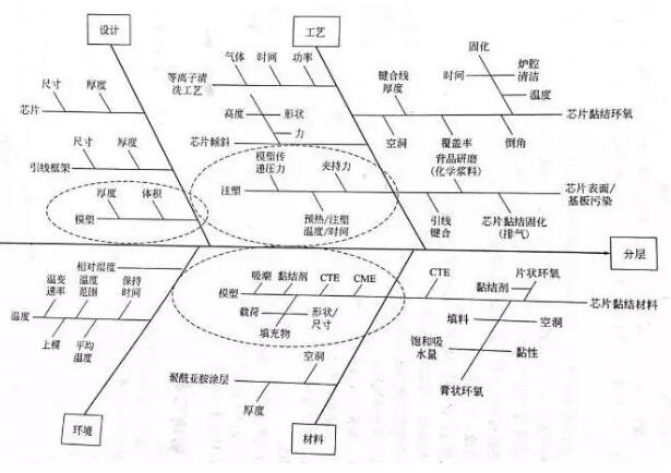
This picture shows the fishbone diagram showing the reasons for the delamination of plastic packaging chips, and it is analyzed from four aspects: design, technology, environment and materials. Through the fishbone diagram, all the influencing factors are clearly displayed, which lays a good foundation for failure analysis.
The load type that caused the failure.
As mentioned in the previous section, the load types of packages can be divided into mechanical, thermal, electrical, radiation and chemical loads.
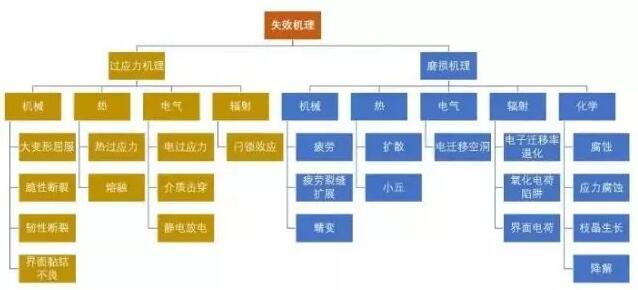
Classification of failure mechanism
Mechanical load: including physical impact, vibration, stress (such as shrinkage stress) and inertial force (such as huge acceleration of spacecraft) exerted by filling particles on the silicon chip, etc. The response of materials to these loads may be manifested as elastic deformation, plastic deformation, warping, brittle or flexible fracture, interface delamination, generation and propagation of fatigue cracks, creep and creep cracking, etc.
Heat load: including the high temperature of die adhesive curing, preheating before wire bonding, molding process, post-curing, reprocessing of adjacent components, immersion welding, gas phase welding and reflow welding, etc. External thermal load will change the size of materials due to thermal expansion, and also change physical properties such as creep rate. For example, thermal expansion coefficient mismatch (CTE mismatch) occurs, which leads to local stress and finally leads to the failure of the packaging structure. Excessive thermal load may even lead to combustion of flammable materials in the device.
Electrical load: including current fluctuation, electrostatic discharge, over-current stress, etc. caused by sudden electrical shock, voltage instability or sudden oscillation during current transmission (such as poor grounding). These external electrical loads may lead to dielectric breakdown, voltage surface breakdown, thermal loss or electromigration of electric energy. It may also increase electrolytic corrosion and dendrite growth, causing leakage current and thermal degradation.
Chemical load: including corrosion, oxidation and ion surface dendrite growth caused by chemical use environment. Because moisture can penetrate through plastic packaging materials, moisture is the main problem affecting plastic packaging devices in humid environment. The moisture absorbed by the plastic packaging material can extract the catalyst residue from the plastic packaging material, forming by-products that enter the metal base, semiconductor materials and various interfaces bonded to the chip, and induce the degradation or even failure of the device performance. For example, the flux remaining on the device after assembly will migrate to the surface of the chip through the plastic package. In high frequency circuits, the subtle changes of dielectric properties (such as the changes of dielectric constant and dissipation factor after moisture absorption) are very critical. In high voltage converters and other devices, the change of breakdown voltage of package is very important. In addition, some epoxy polyamides and polyurethanes will be degraded (sometimes called "reversal") if exposed to high temperature and high humidity for a long time. Usually, accelerated tests are used to identify whether plastic packaging materials are prone to this kind of failure.
It should be noted that when different types of loads are applied, various failure mechanisms may interact on plastic packaging devices at the same time. For example, thermal load will cause thermal expansion coefficient mismatch between adjacent materials in the package structure, which will cause mechanical failure. Other interactions include stress-assisted corrosion, stress corrosion cracking, field-induced metal migration, cracks in passivation layer and electrolyte layer, package cracking caused by damp heat, and chemical reaction acceleration caused by temperature, etc. In these cases, the comprehensive effects of failure mechanisms are not necessarily equal to the sum of individual effects.
Classification of packaging defects
Packaging defects mainly include lead deformation, pedestal deviation, warpage, chip cracking, delamination, voids, uneven packaging, burrs, foreign particles and incomplete curing.
Lead wire deformation
The lead deformation usually refers to the displacement or deformation of the lead caused by the flow of the plastic sealing material, which is usually expressed by the ratio x/L between the maximum lateral displacement x of the lead and the length l of the lead. Bending leads may cause electrical short circuit (especially in high-density I/O device packages). Sometimes, the stress caused by bending will lead to cracking of bonding points or decrease of bonding strength.
Factors affecting wire bonding include package design, wire layout, wire material and size, properties of molding compound, wire bonding process and packaging process, etc. The wire parameters that affect the wire bending include wire diameter, wire length, wire breaking load, wire density and so on.
Base offset
The offset refers to the deformation and offset of the carrier (chip base) supporting the chip.
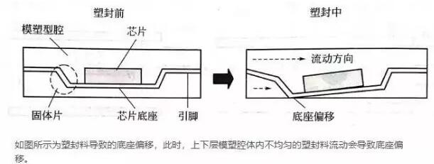
As shown in the figure, the base offset caused by the molding compound. At this time, the uneven flow of the molding compound in the upper and lower molding cavities will cause the base offset.
The factors affecting the offset of the base include the fluidity of the plastic package, the assembly design of the lead frame and the material properties of the plastic package and the lead frame. Packaging devices such as TSOP and TQFP are prone to base offset and pin deformation due to the thin lead frame.
warping
Warping refers to the bending and deformation of packaged devices out of plane. The warpage caused by plastic packaging process will lead to a series of reliability problems such as delamination and chip cracking. Warping will also lead to a series of manufacturing problems. For example, in plastic ball grid array (PBGA) devices, warping will lead to poor coplanarity of solder balls, which will lead to mounting problems in the reflow soldering process of the devices assembled to printed circuit boards.
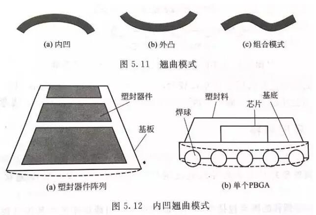
Warping modes include concave, convex and combined modes.
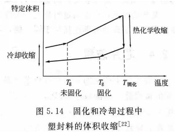
The causes of warpage mainly include CTE mismatch and curing/compression shrinkage. At first, the latter did not receive much attention. In-depth research found that the chemical shrinkage of molding compound also played an important role in the warpage of IC devices, especially on the packaging devices with different thicknesses on the upper and lower sides of the chip. In the process of curing and post-curing, the chemical shrinkage of plastic packaging material will occur at high curing temperature, which is called "thermochemical shrinkage". By increasing the glass transition temperature and decreasing the change of thermal expansion coefficient near Tg, the chemical shrinkage during curing can be reduced.
The factors leading to warpage also include ingredients of molding compound, moisture of molding compound, geometric structure of package, etc. By controlling the materials and components of plastic packaging, process parameters, packaging structure and pre-packaging environment, packaging warpage can be minimized. In some cases, the warpage can be compensated by packaging the back of electronic components. For example, the external connections of large ceramic circuit boards or multilayer boards are located on the same side, and back packaging them can reduce warpage.
Chip rupture
The stress generated in the packaging process will cause the chip to crack. The packaging process usually aggravates the microcracks formed in the previous assembly process. Or wafer chip thinning, back grinding and chip bonding are all steps that may lead to chip crack initiation.
Cracked and mechanically failed chips do not necessarily have electrical failures. Whether the chip crack will lead to the instantaneous electrical failure of the device also depends on the growth path of the crack. For example, if the crack appears on the back of the chip, it may not affect any sensitive structure.
Because silicon wafers are thin and brittle, chip cracking is more likely to occur in wafer-level packages. Therefore, the process parameters such as clamping pressure and molding conversion pressure in transfer molding process must be strictly controlled to prevent the chip from cracking. Chip cracking is easy to occur in 3D stacked package due to lamination process. The design factors that affect chip breakage in 3D packaging include chip stack structure, substrate thickness, molding volume, mold sleeve thickness, etc.
layer
Or weak delamination refers to the separation between the plastic sealing compound and its adjacent material interface. The delamination position may occur in any area in the plastic package microelectronic device; It may also occur in the packaging process, post-packaging manufacturing stage or device use stage.
The poor bonding interface caused by packaging is the main factor causing delamination. Interface voids, surface contamination during packaging and incomplete curing will all lead to poor bonding. Other influencing factors include shrinkage stress and warpage during curing and cooling. During the cooling process, the CTE mismatch between the molding compound and adjacent materials will also lead to thermo-mechanical stress, which will lead to delamination.
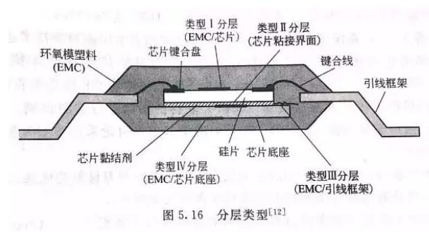
Layers can be classified according to the interface type:
cavity
In the packaging process, bubbles are embedded in epoxy materials to form voids, which can occur at any stage of the packaging process, including transfer molding, filling, potting and printing of plastic packaging materials in air environment. By minimizing the amount of air, such as emptying or vacuuming, the voids can be reduced. It has been reported that the vacuum pressure range is 1~300Torr (one atmospheric pressure is 760Torr).
According to the simulation analysis, it is the contact between the front of the bottom melt and the chip that hinders the fluidity. Part of the front edge of the melt flows upward and fills the top of the mold half through the large open area around the chip. The newly formed melt front and the adsorbed melt front enter the top area of the mold half, thus forming bubbles.
Uneven packaging
Non-uniform thickness of plastic package will lead to warpage and delamination. Traditional packaging technologies, such as transfer molding, pressure molding and pouring packaging technology, are not easy to produce packaging defects with uneven thickness. Wafer-level packaging is easy to cause uneven plastic packaging thickness because of its technological characteristics.
In order to obtain uniform thickness of plastic sealing layer, the wafer carrier should be fixed with minimum inclination to facilitate the installation of scraper. In addition, it is necessary to control the position of the scraper to ensure that the pressure of the scraper is stable, so as to obtain a uniform thickness of the plastic sealing layer.
Before hardening, when the filler particles gather and form uneven distribution in the local area of the plastic sealing compound, it will lead to different quality or uneven material composition. Inadequate mixing of plastic packaging materials will lead to different quality phenomena in the process of packaging and potting.
rough selvedge
The raw edge refers to the molding compound that passes through the molding line and is deposited on the pin of the device in the plastic packaging process.
Insufficient clamping pressure is the main cause of burrs. If the mold residue on the pins is not removed in time, it will lead to various problems in the assembly stage. For example, insufficient bonding or adhesion in the next packaging stage. Resin leakage is a sparse form of burrs.
Exotic particles
In the packaging process, if the packaging materials are exposed to the polluted environment, equipment or materials, foreign particles will diffuse in the packaging and gather on the metal parts in the packaging (such as IC chips and wire bonding points), which will lead to corrosion and other subsequent reliability problems.
Incomplete curing
Insufficient curing time or low curing temperature will lead to incomplete curing. In addition, in the pouring of the two potting materials, the slight deviation of the mixing ratio will lead to incomplete curing. In order to maximize the characteristics of packaging materials, it is necessary to ensure that the packaging materials are completely cured. In many packaging methods, post-curing is allowed to ensure the complete curing of packaging materials. Moreover, attention should be paid to ensuring the accurate proportion of packaging materials.
Classification of package failure
Package failure will occur at the stage of package assembly or device use. Especially when the packaged microelectronic device is assembled on the printed circuit board, it is more likely to happen. At this stage, the device needs to bear high reflow temperature, which will lead to delamination or cracking of the interface of the plastic packaging material.
layer
As mentioned in the previous section, delamination refers to the separation of plastic packaging materials from adjacent materials at the bonding interface. External loads and stresses that may lead to delamination include water vapor, moisture, temperature and their combined effects.
A kind of delamination that often occurs in the assembly stage is called water vapor induced delamination, and its failure mechanism is mainly water vapor pressure at relatively high temperature. When the package device is assembled on the printed circuit board, the melting temperature of the solder needs to reach 220℃ or even higher, which is much higher than the glass transition temperature of the molding compound (about 110~200℃). At high reflow temperature, the water vapor existing between the plastic packaging material and the metal interface evaporates to form water vapor, and the generated vapor pressure acts together with factors such as thermal mismatch between materials, stress caused by moisture absorption and expansion, etc., which eventually leads to weak bonding or delamination of the interface, and even leads to the rupture of the package. Compared with traditional lead-based solders, lead-free solders have higher reflow temperature and are more prone to delamination.
Moisture absorption expansion coefficient (CHE), also known as moisture expansion coefficient (CME)
The failure mechanism of moisture diffusion to packaging interface is an important factor of delamination caused by water vapor and moisture. Moisture can diffuse through the package or along the interface between the lead frame and the molding compound. It is found that when the interface between molding compound and lead frame is well bonded, moisture mainly enters the package through the plastic package. However, when this bonding interface degrades due to poor packaging technology (such as oxidation caused by bonding temperature, lead frame warping caused by insufficient stress release, excessive trimming and formal stress, etc.), delamination and micro-cracks will be formed on the packaging outline, and moisture or water vapor will easily spread along this path. Worse, moisture will lead to hydration of polar epoxy adhesive, which will weaken and reduce the chemical bonding at the interface.
Clean surface is the key requirement to achieve good adhesion. Surface oxidation often leads to delamination (as mentioned in the previous article). For example, copper alloy lead frames exposed to high temperature often lead to delamination. The existence of nitrogen or other synthetic gas is beneficial to avoid oxidation.
Lubricants and adhesion promoters in plastics can promote delamination. Lubricant can help the molding compound to separate from the mold cavity, but it will increase the risk of interface delamination. On the other hand, adhesion promoter can ensure good adhesion between molding compound and chip interface, but it is difficult to remove from the mold cavity.
Layering not only provides a path for water vapor diffusion, but also is the source of resin cracks. The interface is the location of crack initiation, and the crack will propagate through the resin when subjected to high external load. The results show that the delamination between the ground of the chip base and the resin is most likely to cause the resin crack, and the interface delamination in other positions has little influence on the resin crack.
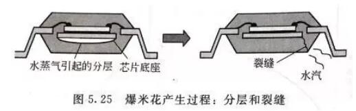
Gas-induced cracking (popcorn phenomenon)
The further development of water vapor induced stratification will lead to gas induced cracking. When the water vapor in the package escapes through the crack, it will produce crackling sound, which is very similar to the sound of popcorn, so it is also called popcorn phenomenon. Cracks often extend from the chip base to the bottom of the plastic package. In the soldered circuit board, it is difficult to find these cracks by visual inspection. Big and thin plastic packaging forms such as QFP and TQFP are most likely to produce popcorn phenomenon; In addition, it is also easy to occur in devices with a large ratio of chip base area to device area and a large ratio of chip base area to minimum plastic sealing material thickness. Popcorn phenomenon may be accompanied by other problems, including the breakage of the bonding ball from the bonding disk and the silicon pits under the bonding ball.
Cracks in plastic packaging devices usually originate from stress concentration areas (such as edges and burrs) on the lead frame, and propagate in the thinnest plastic packaging area. It is the small-size deformation of the surface of the lead frame produced in the stamping process. Changing the stamping direction so that the burrs are located on the top of the lead frame or etching the lead frame (die pressing) can reduce the cracks.
Reducing moisture in plastic packaging devices is the key to reduce popcorn phenomenon. Adopt the method of baking at high temperature to reduce the moisture in the plastic package device. Previous studies have found that the allowable safe moisture content in the package is about 1100× 10^-6(0.11 wt.%)。 Baking at 125℃ for 24h can fully remove the moisture absorbed in the package.
brittle fracture
Brittle fracture often occurs in low yield strength and inelastic materials (such as silicon chips). When the material is overstressed, sudden and catastrophic crack propagation will originate from tiny defects such as voids, inclusions or discontinuities.
ductile fracture
Plastic packaging materials are prone to brittle and ductile fracture modes, which mainly depend on environmental and material factors, including temperature, viscoplastic characteristics of polymer resin and filling load. Even in high-load plastic packaging materials containing brittle silicon filler, ductile fracture may still occur due to the viscoplastic characteristics of polymer resin.
fatigue crack
When the plastic sealing material is subjected to the cyclic stress within the limit strength range, it will break due to the accumulated fatigue fracture. The wet, thermal, mechanical or comprehensive loads applied to the plastic packaging materials will all produce cyclic stress. Fatigue failure is a kind of wear failure mechanism, and cracks usually originate at discontinuous points or defect positions.
The fatigue mechanism includes three stages: crack initiation (stage ⅰ); Stable crack propagation (stage Ⅱ); Sudden, uncertain and catastrophic failure (stage III). Under cyclic stress, fatigue crack propagation in stage ⅱ refers to the steady growth of crack length. The crack growth rate of plastic packaging materials is much higher than the typical value of fatigue crack growth of metal materials (about 3 times).
Factors that accelerate failure
And the load and stress of environmental materials, such as moisture, temperature and pollutants, will accelerate the failure of plastic packaging devices. Plastic packaging technology is playing a key role in packaging failure, such as moisture diffusion coefficient, saturated moisture content, ion diffusion rate, thermal expansion coefficient and moisture absorption expansion coefficient of plastic packaging materials, which will greatly affect the failure rate. Factors leading to accelerated failure mainly include moisture, temperature, pollutants and solvent environment, residual stress, natural environmental stress, manufacturing and assembly loads and comprehensive load stress conditions.
Moisture can accelerate delamination, crack and corrosion failure of plastic encapsulated microelectronic devices. Moisture is an important failure accelerating factor in plastic packaging devices. The mechanisms related to the failure acceleration caused by moisture include the degradation of bonding surface, moisture absorption and expansion stress, water vapor pressure, ion migration, and the change of characteristics of plastic packaging materials.
Moisture can change the glass transition temperature Tg, elastic modulus and volume resistivity of plastic packaging materials.Temperature is another key failure accelerating factor. Usually, the temperature grade related to the glass transition temperature of molding compound, thermal expansion and washing of various materials and the thermal-mechanical stress caused by it is used to evaluate the effect of temperature on package failure. Another influence factor of temperature on packaging failure is that it will change the properties of packaging materials, moisture diffusion coefficient and intermetallic diffusion related to temperature.
Contaminants and solvent environmental pollutants provide a place for the initiation and expansion of failures. Pollution sources mainly include air pollutants, moisture, flux residues, unclean examples in plastic packaging materials, corrosive elements produced by thermal degradation and by-products (usually epoxy) discharged from chip adhesives. Generally, the plastic package will not be corroded, but moisture and pollutants will diffuse in the plastic package and reach the metal parts, causing corrosion of the metal parts in the plastic package devices.
Residual stress chip bonding will produce unit stress. The stress level mainly depends on the characteristics of the bonding layer of the chip. Because the shrinkage of molding compound is larger than that of other packaging materials, the stress generated during molding is quite large. The stress test chip can be used to measure the assembly stress.
Environmental stress In the natural environment, plastic packaging materials may be degraded. The degradation is characterized by the breakage of polymerization bonds, and it is often that solid polymers are converted into viscous liquids containing monomers, dimers and other low molecular weight species. Elevated temperature and closed environment often accelerate degradation. Ultraviolet rays in sunlight and atmospheric ozone layer are powerful catalysts for degradation, which can lead to degradation by cutting off the molecular chain of epoxy resin. Isolating the plastic packaging device from the environment which is easy to induce degradation, and adopting polymers with anti-degradation ability are the methods to prevent degradation. Products that need to work in hot and humid environment require anti-degradation polymers.
Manufacturing and assembly load The manufacturing and assembly conditions may lead to package failure, including high temperature, low temperature, temperature change, operating load, and the load exerted on bonding wires and chip base due to the flow of plastic sealing material. The popcorn phenomenon during the assembly of plastic packaging devices is a typical example.
Comprehensive load stress conditions In the process of manufacture, assembly or operation, failure acceleration factors such as temperature and moisture often exist simultaneously. Combined load and stress conditions often further accelerate failure. This feature is often applied to the accelerated test design for the purpose of screening defective parts and identifying vulnerable packaged devices.
Brief introduction of failure analysis
Generally, according to failure modes and phenomena, it simulates the activities of reappearing failure phenomena, finding out the causes of failure and digging out the mechanism of failure through analysis and verification. It is of great practical significance in improving product quality, technology development and improvement, product repair and arbitration of failure accidents.
Failure analysis process
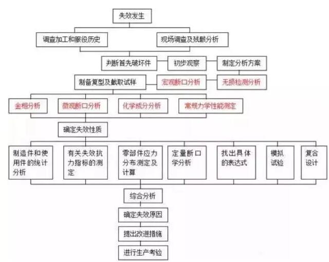
图1 Failure analysis process
Failure analysis and detection method of various materials
1. PCB/PCBA failure analysis
As the carrier of various components and the hub of circuit signal transmission, PCB has become the most important and critical part of electronic information products, and its quality and reliability level determine the quality and reliability of the whole equipment.
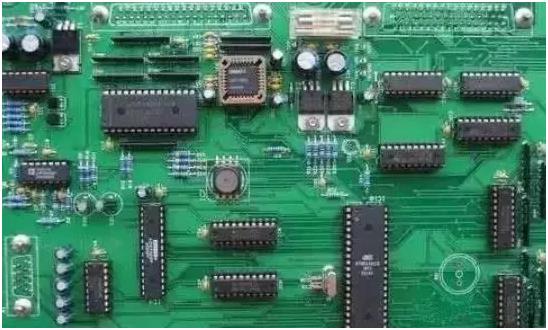
图2 PCB/PCBA
failure mode
Plate explosion, delamination, short circuit, blistering, poor welding, corrosion migration, etc.
Common means
Non-destructive testing:
Appearance inspection, X-ray fluoroscopy inspection, 3D CT inspection, C-SAM inspection, infrared thermal imaging
Surface element analysis:
Scanning electron microscope and energy spectrum analysis (SEM/EDS)
Micro-infrared analysis (FTIR)
Auger electron spectroscopy (AES)
X-ray photoelectron spectroscopy (XPS)
Secondary ion mass spectrometry (TOF-SIMS)
Thermal analysis:
Differential scanning calorimetry (DSC)
Mechanical analysis (TMA)
Thermal analysis (TGA)
Dynamic mechanical analysis (DMA)
Thermal conductivity (steady-state heat flow method, laser scattering method)
Electrical performance test:
Breakdown voltage, withstand voltage, dielectric constant, electromigration
Destruction performance test:
Dyeing and penetrant detection
2. Failure analysis of electronic components
The rapid development of electronic component technology and the improvement of reliability have laid the foundation of modern electronic equipment. The fundamental task of component reliability work is to improve the reliability of components.

Figure 3 Electronic components
failure mode
Open circuit, short circuit, electric leakage, functional failure, electrical parameter drift, unstable failure, etc.
Common means
Electrical measurement: connectivity test, electrical parameter test and functional test.
Non-destructive testing:
Opening technology (mechanical opening, chemical opening, laser opening)
Passivation technology (chemical etching, plasma etching, mechanical grinding)
Micro-analysis technology (FIB, CP)
Sample preparation technology:
Opening technology (mechanical opening, chemical opening, laser opening)
Passivation technology (chemical etching, plasma etching, mechanical grinding)
Micro-analysis technology (FIB, CP)
Microscopic morphology analysis:
Optical analysis technologySecondary electron image technology of scanning electron microscope
Surface element analysis:
Scanning electron microscope and energy spectrum analysis (SEM/EDS)
Auger electron spectroscopy (AES)
X-ray photoelectron spectroscopy (XPS)
Secondary ion mass spectrometry (SIMS)
Nondestructive analysis technology:
X-ray fluoroscopyThree-dimensional perspective technologyReflective scanning acoustic microscopy (C-SAM)
3.Material failure analysis
With the progress of society and the development of science and technology, metal products are widely used in industry, agriculture, science and technology and people's life, so the quality of metal materials should be paid more attention to.
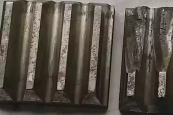
Figure 4 Crankshaft gear of marine diesel engine
failure mode
Improper design, material defects, casting defects, welding defects and heat treatment defects.
Common means
Material microstructure analysis:
metallographic analysis
X-ray phase structure analysis
Surface residual stress analysis
Grain size of metal
Composition analysis: direct reading spectrometer, X-ray photoelectron spectroscopy (XPS), Auger electron spectroscopy (AES), etc.
Phase analysis: X-ray diffraction (XRD)
Residual stress analysis: X-ray stress tester
Mechanical performance analysis: universal testing machine, impact testing machine, hardness testing machine, etc.
Mechanical performance analysis: universal testing machine, impact testing machine, hardness testing machine, etc.
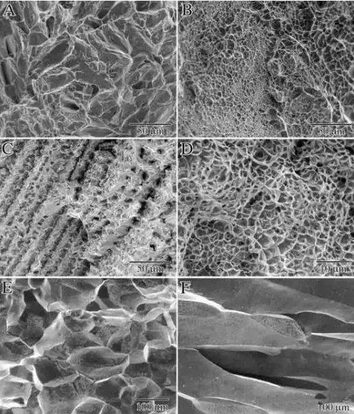
Fig. 5 SEM image of fracture surface of tensile test material
4. Failure analysis of polymer materials
The general development trend of polymer technology is high-performance, high-functionality, complex, intelligent and green. Because of the brand-new requirements of technology and the high demand of products, it is necessary to find the root cause and mechanism of its failure by means of failure analysis to improve product quality, process improvement and liability arbitration.
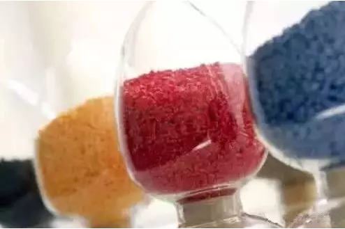
Figure 6 Spray-free plastics
failure mode
Fracture, cracking, delamination, corrosion, blistering, coating shedding, discoloration and wear failure.
Common means
Composition analysis:
Fourier transform infrared spectrometer (FTIR)
Microscopic confocal Raman spectrometer (Raman)
Scanning electron microscope and energy spectrum analysis (SEM/EDS)
X-ray fluorescence spectrometry (XRF)
Gas chromatography-mass spectrometry (GC-MS)
Pyrolysis gas chromatography-mass spectrometry (PGC-MS)
Nuclear magnetic resonance analysis (NMR)Auger electron spectroscopy (AES)
X-ray photoelectron spectroscopy (XPS)
X-ray diffractometer (XRD)
Time-of-flight secondary ion mass spectrometry (TOF-SIMS)
Thermal analysis:
Differential scanning calorimetry (DSC)
Mechanical analysis (TMA)
Thermal analysis (TGA)
Dynamic mechanical analysis (DMA)
Thermal conductivity (steady-state heat flow method, laser scattering method)
Cracking analysis:
Pyrolysis gas chromatography-mass spectrometryGel permeation chromatography (GPC)
Melt index test (MFR)
Fracture analysis:
Scanning electron microscope (SEM), x-ray energy spectrometer (EDS), etc.
Physical performance analysis:
Hardness tester, tensile tester, universal tester, etc.
5. Failure analysis of composite materials
Composite material is a combination of two or more materials with different properties. It has the advantages of high specific strength, excellent toughness and good environmental resistance, so it is widely used in practical production.
failure mode
Fracture, discoloration failure, corrosion, insufficient mechanical properties, etc.
Common means
Non-destructive testing:
X-ray detection technology (X-ray, γ-ray, neutron ray, etc.), industrial CT, Compton backscattering imaging (CST) technology, ultrasonic detection technology (penetration method, pulse reflection method, tandem method), infrared thermal wave detection technology, acoustic emission detection technology, eddy current detection technology, microwave detection technology, laser holographic detection technology, etc.
Composition analysis:
X-ray fluorescence spectrometry (XRF), etc., see composition analysis in failure analysis of polymer materials.
Thermal analysis:
Gravimetric analysis (TG), differential scanning calorimetry (DSC), static thermomechanical analysis (TMA), dynamic thermomechanical analysis (DMTA) and dynamic dielectric analysis (DETA).
Destructive experiment:
Analysis (metallographic section, focused ion beam (FIB) sample preparation, ion milling (CP) sample preparation)
6. Failure Analysis of Coating/Coating
failure mode
Delamination, cracking, corrosion, blistering, coating/plating falling off, discoloration failure, etc.
Common means
Composition analysis:
See failure analysis of polymer materials.
Thermal analysis:
See failure analysis of polymer materials.
Fracture analysis:
Volume microscope (OM)Scanning electron microscope analysis (SEM)
Physical properties:
Tensile strength, bending strength, etc.
Simulation test (if necessary)
Test under the same working condition, or test under simulated working condition.
Analysis result submission
1) put forward the nature and cause of failure.
2) Put forward preventive measures (suggestions)
3) Submit failure analysis report.
Summary: Failure analysis is a combination of experience and science. Fault engineers are like doctors. At the beginning of process design, preventive measures should be taken; After the product leaves the factory, physical examination is carried out to find hidden dangers and preventive measures. Give the measured value; Find the cause by various means: blood test, X-ray, B-ultrasound, etc. According to the inspection data, analyze the symptoms, prescribe the right medicine and give remedial measures.
Summary: Failure analysis is a combination of experience and science. Fault engineers are like doctors. At the beginning of process design, preventive measures should be taken; After the product leaves the factory, physical examination is carried out to find hidden dangers and preventive measures. Give the measured value; Find the cause by various means: blood test, X-ray, B-ultrasound, etc. According to the inspection data, analyze the symptoms, prescribe the right medicine and give remedial measures.
Site Map | 萨科微 | 金航标 | Slkor | Kinghelm
RU | FR | DE | IT | ES | PT | JA | KO | AR | TR | TH | MS | VI | MG | FA | ZH-TW | HR | BG | SD| GD | SN | SM | PS | LB | KY | KU | HAW | CO | AM | UZ | TG | SU | ST | ML | KK | NY | ZU | YO | TE | TA | SO| PA| NE | MN | MI | LA | LO | KM | KN
| JW | IG | HMN | HA | EO | CEB | BS | BN | UR | HT | KA | EU | AZ | HY | YI |MK | IS | BE | CY | GA | SW | SV | AF | FA | TR | TH | MT | HU | GL | ET | NL | DA | CS | FI | EL | HI | NO | PL | RO | CA | TL | IW | LV | ID | LT | SR | SQ | SL | UK
Copyright ©2015-2025 Shenzhen Slkor Micro Semicon Co., Ltd
