Service hotline
+86 0755-83044319

release time:2022-03-17Author source:SlkorBrowse:13848
一、3D packaging will be the main process.
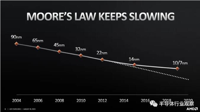
Recently, Yang Rui, research director of [敏感词] Province Institute of Industrial Technology in China, predicted that [敏感词] will dominate the chip manufacturing industry for another five years, after which 3D packaging will become the main process challenge.In the past decade, various computing workloads have developed rapidly, but Moore's Law has been repeatedly spread and will come to an end. Faced with more diverse computing application requirements, in order to "plug" more functions into the same chip, advanced packaging technology has become the key innovation path to continuously optimize the performance and cost of the chip.[敏感词], Intel and Samsung are all accelerating the deployment of 3D packaging technology. In August of this year, all three chip manufacturing giants showed up, making this battlefield more and more smoky.
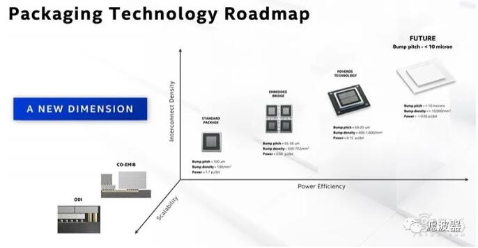
▲Intel Packaging Technology Roadmap
Through the advanced packaging layout of the three chip manufacturing giants, we can see that in the next year, 3D packaging technology will be an important killer beyond Moore's Law.
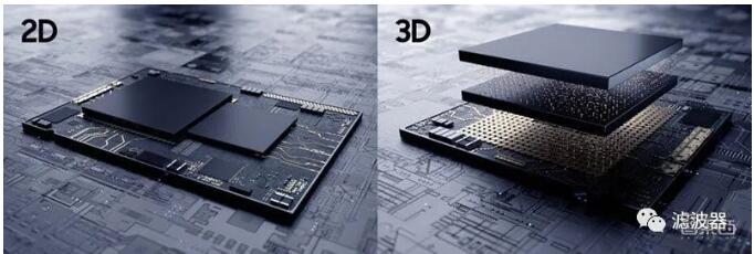
First, advanced packaging: cram more functions into one chip.
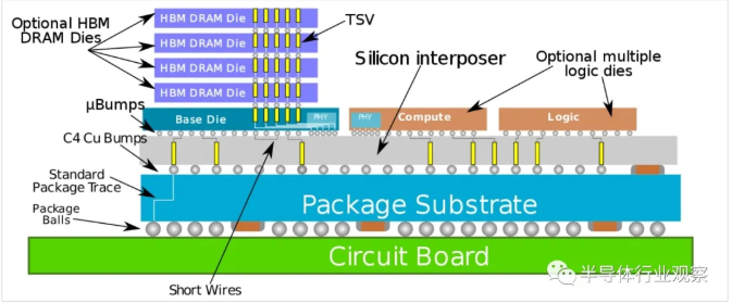
Previously, 2D planar packaging technology was mostly used for chips, but with the increasing demand of heterogeneous computing applications, 3D packaging technology, which can integrate chips of different sizes, processes and materials, has become a necessary choice with higher performance and flexibility.
According to the progress of the latest 3D packaging technology, Intel Lakefield adopts 3D packaging technology Foveros, [敏感词]'s 3D packaging technology SoIC will be mass-produced in 2021 as originally planned, and Samsung's 3D packaging technology has been applied to 7nm EUV chips.
Why move towards advanced packaging technology? There are two main reasons. First, most of the performance limitations of processors come from memory bandwidth, and second, productivity increases.
On the one hand, the development speed of memory bandwidth is far lower than that of processor logic circuit, so there is the problem of "memory wall".
In the traditional PCB package, it is difficult to improve the wiring density and signal transmission rate, so the memory bandwidth increases slowly. However, the advanced packaging has a short wiring density, a large room for signal transmission rate improvement, and can greatly increase the interconnection density, so advanced packaging technology has become one of the main methods to solve the memory wall problem.
On the other hand, the architecture of high-performance processors is becoming more and more complex, and the number of transistors is also increasing, but the advanced semiconductor technology is still expensive and the productivity is not satisfactory.
In semiconductor manufacturing, the smaller the chip area, the higher the yield. In order to reduce the cost of using advanced semiconductor technology and improve the yield, an effective method is to cut the big chip into several small chips, and then use advanced packaging technology to connect them together.In this context, the three chip giants represented by [敏感词], Intel and Samsung are actively exploring 3D packaging technology and other advanced packaging technologies.
Second, [敏感词]'s 3D packaging combination boxing
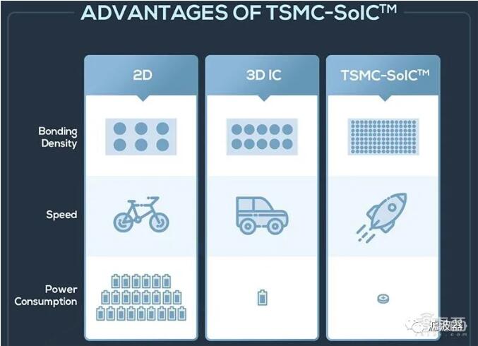
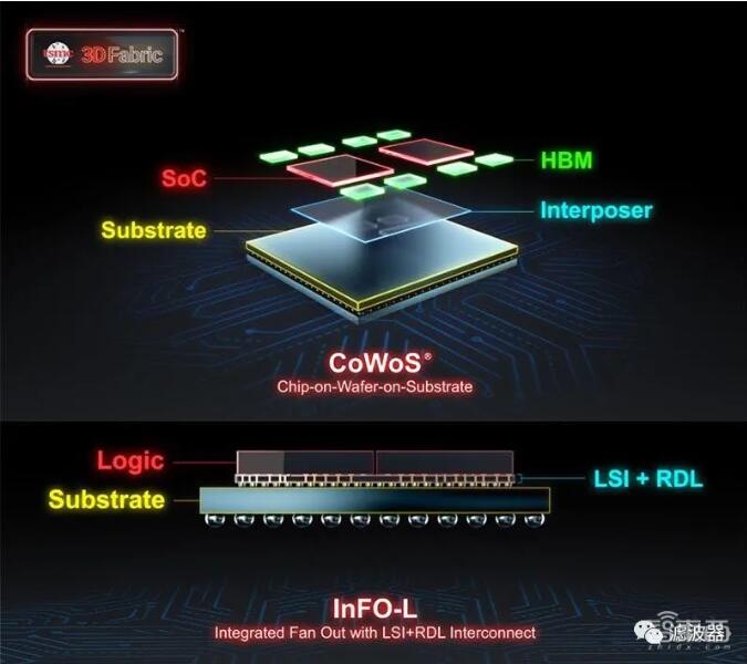
At the end of August this year, [敏感词] launched the 3DFabric integration technology platform, aiming at speeding up the innovation of system-level solutions and shortening the time to market.[敏感词] 3DFabric can integrate various logic, memory devices or special chips with SoC, providing smaller chips for high-performance computers, smart phones, IoT edge devices and other applications, and can improve bandwidth, delay and power efficiency by integrating high-density interconnection chips into package modules.3DFabric consists of [敏感词] front-end and back-end packaging technologies.The front-end IC technology is [敏感词] SoIC technology, which was first announced in 2018, and supports CoW(Chip on Wafer) and WoW(Wafer on Wafer) bonding methods.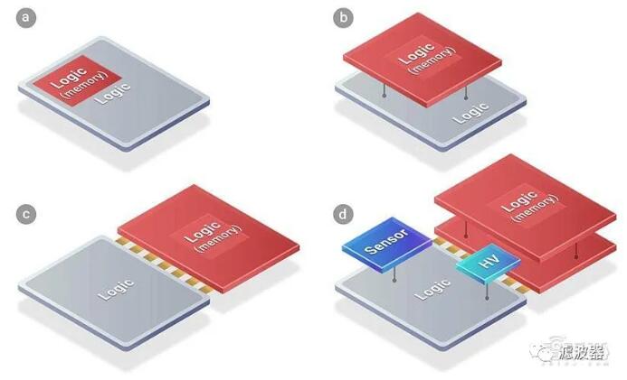
▲ A is the SoC; before chip division; B, C and D are various partition chiplets and re-integration schemes supported by [敏感词] SoIC service platform.
By using silicon via (TSV) technology, [敏感词]'s SoIC technology can achieve a bump-free bonding structure, so that small chips with different sizes, processes and materials can be re-integrated into an integrated chip similar to SoC, making the final integrated chip smaller in area and the system performance better than the original SoC.
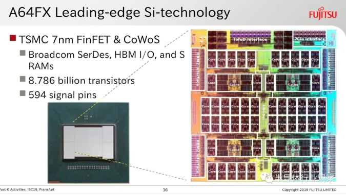
[敏感词]'s back-end technologies include CoWoS(Chip on Wafer on Substrate) and InFO(Integrated Fan-out) series of packaging technologies, which have been widely used. For example, Fujitsu A64FX processor carried by Japanese supercomputer "Fuyue", which ranks first in the global TOP 500 supercomputer list this year, adopts [敏感词] CoWoS packaging technology, and Apple's mobile phone chip adopts [敏感词] InFO packaging technology.
In addition, [敏感词] has several specialized back-end fabs, which are responsible for assembling and testing silicon chips, including 3D stacked chips, and processing them into packaged devices.
One of the great benefits of this is that customers can adopt more mature and lower-cost semiconductor technologies in modules that do not change frequently, such as analog IO, RF, etc., and adopt the most advanced semiconductor technologies in core logic design, which not only saves costs, but also shortens the time to market of new products.
[敏感词] 3DFabric integrates advanced logic and high-speed memory devices into the package module. In a given bandwidth, the wider interface of HBM enables it to run at a lower clock speed, thus reducing power consumption.
In terms of data center scale, the cost savings of these logic and HBM devices are considerable.
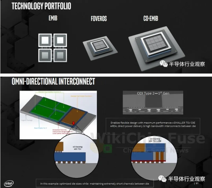
Third, Intel uses the "decomposition design" strategy to play a differentiated advantage.Similar to [敏感词], Intel has already laid out advanced packaging technologies with multiple dimensions in the field of packaging.
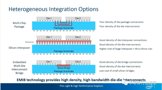
On August 13th, 2020 Intel Architecture Day, Intel released a brand-new Integrated Fan-out technology, and the test chips using this technology were streamed in the second quarter of 2020.Compared with the Thermocompression bonding technology used by most packaging technologies, the hybrid bonding technology can reduce the bump pitch to less than 10 microns, providing higher interconnection density, higher bandwidth and lower power.
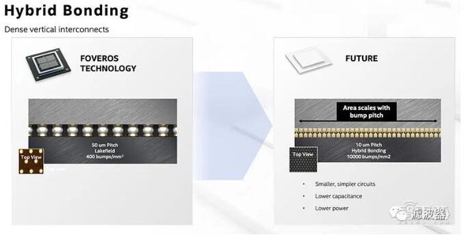
▲Intel hybrid bonding technology
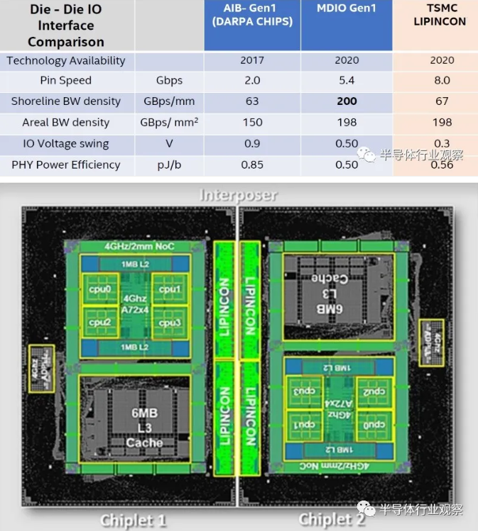
Intel has previously introduced standard package, 2.5D embedded multi-interconnect bridge (EMIB) technology, 3D packaged Foveros technology, Co-EMIB technology combining EMIB with Foveros technology, Omni-directional Interconnection (ODI) technology and multi-mode I/O(MDIO) technology, etc. These package interconnection technologies can bring greater scalability and flexibility when superimposed on each other.
According to Song Jiqiang, president of Intel Research Institute, "The development of packaging technology is like building a house. At first, we built a cottage room, then we built a quadrangle, and finally we built a high-rise building. In the case of Foveros 3D, what it achieves is that when building tall buildings, it can make the lines transmit at low power and high speed. "He believes that Intel's advantage in packaging technology is that it can know earlier how this house will be built in the future, that is to say, it can better design future chips.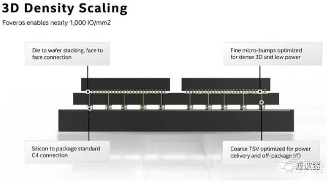
Facing the future trend of heterogeneous computing, Intel introduced the strategy of "Decomposition Design", which combined with new design methods and advanced packaging technology to split the key architecture components into individual chips still in unified packaging.
That is to say, the original whole SoC chip will be "broken into parts", first made into several major parts, such as CPU, GPU, I/O, etc., and then the fine-grained SoC will be further improved, and the previous idea of combining according to functionality will be changed to combining according to chip IP.
The advantage of this idea is that it can not only improve the efficiency of chip design, reduce the production time, but also effectively reduce the number of bugs caused by previous complex designs.
"The original scheme that must be made on one chip can now be converted into multi-chips. In addition, you can not only use Intel's multi-node process technology, but also the technology of partners. " Song jiqiang explained.After these decomposed widgets are integrated, they have high speed, sufficient bandwidth, low power consumption and great flexibility, which will become a big difference advantage of Intel.
Fourth, Samsung's first 3D packaging technology can be used in 7nm process.Besides [敏感词] and Intel, Samsung is also accelerating the deployment of its 3D packaging technology.
On August 13th, Samsung also announced that its 3D packaging technology is "eXtended-Cube", referred to as "X-Cube" for short. It is interconnected by TSV and can be used in 7nm or even 5nm processes.According to Samsung, at present, its X-Cube test chip can stack the SRAM layer on the logic layer, which can separate the SRAM from the logic part, thus freeing up more space to stack more memory.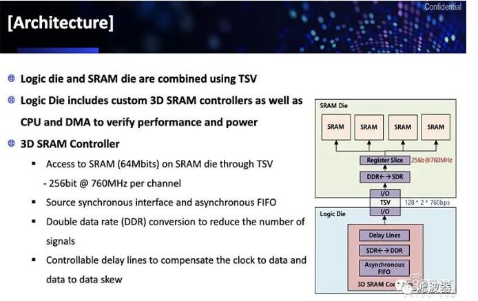
▲X-Cube test chip architecture of Samsung
二、Chip giant decides advanced packaging
From: semiconductor industry observation
Development of advanced packaging technology in the ascendant

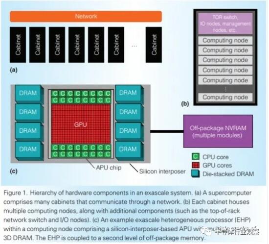
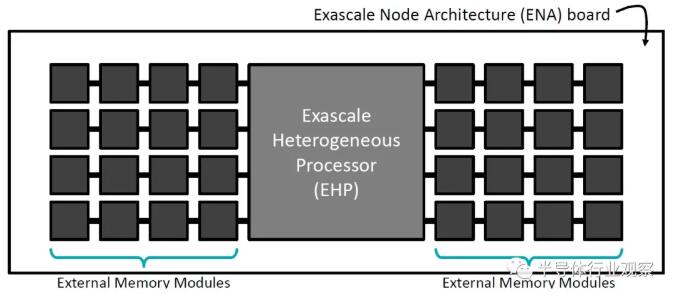
System-on-a-chip for supercomputers is not a patent of IBM and Fujitsu.
There are 8 32 GPU CU, totaling 256 CU and 16,384 streaming processors (Vega, which was scheduled to be the fifth generation of GCN at that time, seems to advance to CDNA).
Eight 4GB HBM2 memory stacks.
When the clock is 1GHz, the theoretical efficiency of double floating-point precision is 16TeraFlops, such as 100,000 supercomputers, which is 1.6ExaFlops, and the estimated power consumption is 20MW.
In July, 2015, AMD published a special article on IEEE Micro, indicating that 32 CPU cores, 320 GPU CUs with 1GHz clock (20,480 streaming processors), 3TB/s memory bandwidth and 160W power consumption are the configurations with the best energy consumption ratio. In short, the actual products will definitely change.
The terrible rumors that the technical assets of EHP and X3D will "push themselves to others" to the Zen 3 generation EPYC processor "Milan" (such as 10 CCDs with 80 cores or HBM2 as L4) have never stopped.
Co-screening: nVidia is not full and idle.
Implication: Impact of GPU Driver Open Source
The development of technology follows the demand of applications, which may also determine whether AMD's attempt to counter-attack the high-performance computing market by means of "supercomputer APU" will be the key to success.
Disclaimer: This article is reproduced from "Filter". This article only represents the author's personal views, not those of Sacco Micro and the industry. It is only for reprinting and sharing, and supports the protection of intellectual property rights. Please indicate the original source and author when reprinting. If there is any infringement, please contact us to delete it.
Company Tel: +86-0755-83044319
Fax/fax:+86-0755-83975897
Email: 1615456225@qq.com
QQ: 3518641314 Manager Li
QQ: 332496225 Manager Qiu
Address: Room 809, Block C, Zhantao Technology Building, No.1079 Minzhi Avenue, Longhua New District, Shenzhen
Site Map | 萨科微 | 金航标 | Slkor | Kinghelm
RU | FR | DE | IT | ES | PT | JA | KO | AR | TR | TH | MS | VI | MG | FA | ZH-TW | HR | BG | SD| GD | SN | SM | PS | LB | KY | KU | HAW | CO | AM | UZ | TG | SU | ST | ML | KK | NY | ZU | YO | TE | TA | SO| PA| NE | MN | MI | LA | LO | KM | KN
| JW | IG | HMN | HA | EO | CEB | BS | BN | UR | HT | KA | EU | AZ | HY | YI |MK | IS | BE | CY | GA | SW | SV | AF | FA | TR | TH | MT | HU | GL | ET | NL | DA | CS | FI | EL | HI | NO | PL | RO | CA | TL | IW | LV | ID | LT | SR | SQ | SL | UK
Copyright ©2015-2025 Shenzhen Slkor Micro Semicon Co., Ltd
