Service hotline
+86 0755-83044319
release time:2022-03-17Author source:SlkorBrowse:10905
1. introduce
With the development of semiconductor chip technology, power devices can effectively use electric energy, such as thyristors and diodes, which play a key role in voltage and current control. Compared with the widely used Si semiconductor chip, the wide bandgap semiconductor SiC chip can improve the product performance and reduce the loss. Compared with traditional devices, SiC devices can reduce the loss by 50-70% and work at higher frequencies. Using SiC devices in the system can reduce the power loss of products and the volume of cooling system and passive components.
The use of SiC power devices can save energy and resources, and mitsubishi electric has been continuously improving its performance and reducing its loss. This paper summarizes the latest development of SiC chips.
2. SiC 芯片的发展
2.1 Second generation planar mosfet
Using our latest 6-inch SiC wafer production line, we have developed the second generation of metal oxide field effect transistors (MOSFETs). For planar gate MOSFETs, the cell structure of MOS is optimized by doping junction field effect transistor, and the on-resistance and capacitance are reduced. For example, fig. 1 shows the conduction characteristics of the second generation planar gate MOSFETs with a withstand voltage of 1200V, and fig. 2 shows the relationship between switching loss and gate resistance. For the convenience of comparison, the curves of the first generation MOSFETs in the same area are also shown in the figure. For the second generation MOSFETs, the on-resistance is reduced by about 15% due to the reduction of cell spacing and other improvement measures. As can be seen from Figure 2, due to the reduction of capacitance and other improvement measures, the switching speed of the second generation MOSFETs is faster and the switching loss is obviously reduced. In addition, the 6-inch SiC wafer production line can make the wafer thinner, thus reducing the on-resistance. Thin wafers have been applied in the second generation planar gate MOSFETs.
At present, we have developed the second generation planar gate MOSFETs with various types of withstand voltages ranging from 600V to 3300V, and successfully commercialized the power modules.
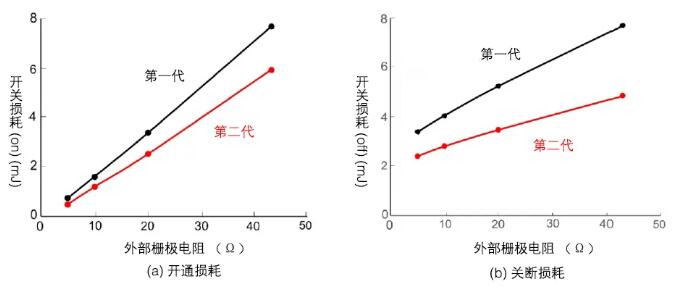
picture1. Second generation plane typeMOSFETConduction characteristic

Figure 2. Switching Loss of the Second Generation Planar Gate MOSFET
2.2 New trench MOSFETs
We have developed a power module equipped with trench gate MOSFETs by adopting a proprietary structure. Due to the physical characteristics of SiC material, the electric field intensity on SiC chip inevitably increases, especially on the gate oxide layer at the bottom of the trench. Therefore, unlike Si trench gate MOSFETs, SiC-MOSFETs need special consideration. Fig. 3 depicts the structure of trench gate MOSFETs developed by us. In order to weaken the electric field intensity acting on the gate oxide layer at the bottom of the trench, a bottom P layer (BPW) is arranged at the lower part of the trench. In order to stabilize the potential of the BPW, P-type dopant ions are obliquely implanted along the sidewall of the trench. At the part of the trench sidewall where the current flows, the angled N-type doping ion implantation can reduce the resistance. Fig. 4 shows the on-resistance of trench gate MOSFETs at room temperature. Figure 5 shows its withstand voltage characteristics. Compared with planar gate MOSFETs, the on-state specific resistance of trench gate MOSFETs is reduced by about 50% at 1.84mΩ·cm2, and the avalanche voltage is designed to be 1560V V.
The low on-resistance characteristic of trench MOSFETs will be used to reduce the chip size, reduce the loss and increase the current level of the module in the future.
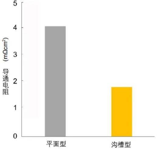
Figure 3. Cross-sectional structure diagram of trench MOSFET

Figure 4. Comparison of on-resistance between planar MOSFET and trench MOSFET
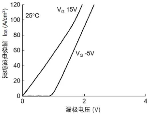
Figure 5. Off-state Characteristics of Trench MOSFET
2.3 MOSFETs MOSFETs SBD integration
There is an internal body diode, because of its structural characteristics, the current can flow through the MOSFETs in the reverse direction, and the body diode can be used as a converter diode. However, for SiC-MOSFETs, when the body diode is turned on, its turn-on voltage drop sometimes increases. For MOSFETs with high withstand voltage and large area, SBD( Schottky Barrier Diode) should be connected in a row as converter diodes, and the body diodes should be screened and tested to avoid the increase of forward voltage drop.
For MOSFETs with a withstand voltage of 3300V or higher, we have developed MOSFETs with built-in SBD chips, whose SBD is built in the unit cell of MOSFETs, without external SBD and body diode screening. When the current flows through MOSFETs with built-in SBD in the reverse direction, the voltage drop caused by the current flowing from the drift layer is lower than the PN junction voltage of the body diode, and the body diode no longer flows the current.
Fig. 6 shows the conduction characteristic curve of MOSFETs with built-in SBD. Its conduction characteristics are similar to those of conventional MOSFETs controlled by gate voltage. Because the electrode area occupied by the built-in SBD is very small, the on-resistance of MOSFET increases very little. Fig. 7 shows the reverse current conduction characteristics of MOSFETs with built-in SBD when the gate voltage of MOSFETs is -5V (off) and 15V (on). The data shows that when the voltage is about 1V (diffusion voltage of SBD), the unipolar current starts to increase linearly. When the gate of the MOSFETs is turned on, the current flowing through the MOSFET channel is superimposed on the SBD current, which obviously reduces the on resistance.
By applying MOSFETs module with built-in SBD, rows of external SBDs can be omitted, which can simplify the test, reduce the size of the module and reduce the cost.

Fig. 6. MOSFET conduction characteristics with built-in SBD

Figure 7. Reverse current conduction characteristics of MOSFET with built-in SBD
conclusion
We will continue to research and develop the second generation planar gate SiC-MOSFETs, trench gate SiC-MOSFETs and SiC-MOSFETs with built-in SBD to further improve the performance of power devices. We hope to use the product characteristics of SiC to reduce the loss of energy and resources in various systems.
Disclaimer: This article is reproduced from "mitsubishi electric Semiconductor". This article only represents the author's personal views, and does not represent the views of Sacco Micro and the industry. It is only for reprinting and sharing to support the protection of intellectual property rights. Please indicate the original source and author when reprinting. If there is any infringement, please contact us to delete it.



Site Map | 萨科微 | 金航标 | Slkor | Kinghelm
RU | FR | DE | IT | ES | PT | JA | KO | AR | TR | TH | MS | VI | MG | FA | ZH-TW | HR | BG | SD| GD | SN | SM | PS | LB | KY | KU | HAW | CO | AM | UZ | TG | SU | ST | ML | KK | NY | ZU | YO | TE | TA | SO| PA| NE | MN | MI | LA | LO | KM | KN
| JW | IG | HMN | HA | EO | CEB | BS | BN | UR | HT | KA | EU | AZ | HY | YI |MK | IS | BE | CY | GA | SW | SV | AF | FA | TR | TH | MT | HU | GL | ET | NL | DA | CS | FI | EL | HI | NO | PL | RO | CA | TL | IW | LV | ID | LT | SR | SQ | SL | UK
Copyright ©2015-2025 Shenzhen Slkor Micro Semicon Co., Ltd