Service hotline
+86 0755-83044319
release time:2022-03-17Author source:SlkorBrowse:10923
As a PCB engineer who has been engaged in PCB design for many years, people often feel bald when they work on drawing boards for a long time. This disturbing pressure, which is neither from the design requirements of the board nor limited by the compatibility between different product structures, really bothers me, is a problem that many engineers will ignore-PCB DFM, that is, the manufacturability analysis and inspection of PCB.
01
What is the problem with PCB DFM? Whether the overall structure of the board meets the production requirements, whether it can meet the batch production conditions of the board factory and whether the production cost can meet the project budgetWait a minute. These questions are full of question marks for most engineers, and they are basically not considered in the design of the board. In the face of the [EQ inquiry] feedback from the factory board factory, it is also a random reply, which eventually leads to the scrap of the finished board and makes it unusable. In the end, it is natural for the engineer to carry the pot himself.
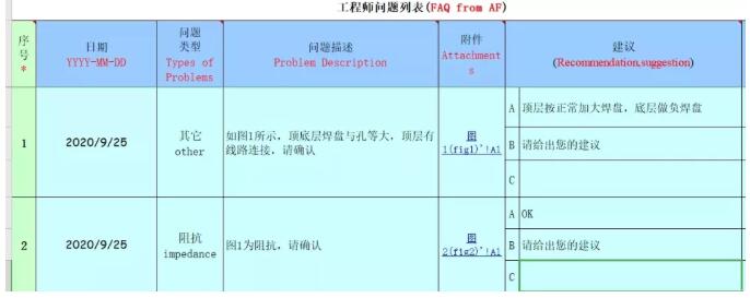
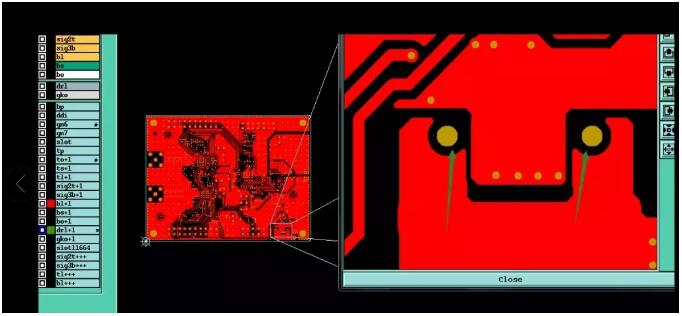
The reason why engineers are behind the scenes is mainly because of such problems, which are the norm in the whole PCB industry. Most PCB design and R&D companies don't set up DFM processes, and engineers don't understand this kind of problems themselves. Just because it is the last mile of the butt board factory, they become professional backers.
Of course, it can't be said that engineers have no responsibility at all. Sometimes it is also a problem of PCB design, as follows:
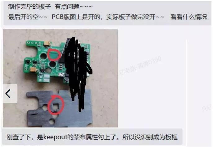
This kind of problem can't be detected by EDA design software. In most cases, it can only be checked by various specification checklists to avoid this kind of problem.
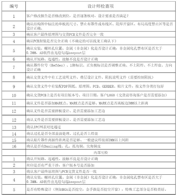
However, manual check often leads to imprecise situation, and if you encounter irresponsible inspectors, there will still be problems with the board in the end.
02
How should PCB DFM be solved?So is there a tool to collect these "PCB inspection items" for automatic inspection?
Actually, there are such softwares, but they are often expensive and have insufficient compatibility (they can only detect files with fixed formats), and the use of piracy may also cause copyright risks. For many enterprises, the cost performance is too low to be considered at all. As a result, there are problems with boards in the industry at present, and then engineers are frequently asked to carry the pot.
Is there such an efficient and free software?
The answer is: yes!
Help PCB engineers solve this industry malady and refuse to take the blame.
Today, I recommend a free and highly compatible PCB design and analysis tool [Huaqiu DFM].
The reason why I recommend this to you is mainly based on years of PCB industry experience. I think it has the following practical functions.
1、Simulation function: It can simulate the effect of real objects, as shown below.
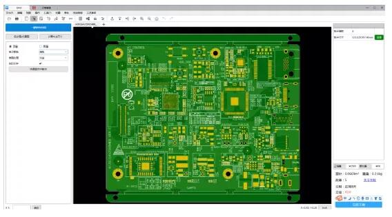
Is this very close to the real thing? Like some problems without drilling holes, you can see it at a glance by looking at this. If there is no rou file, then what you see in the hole is blocked.
2. PCB defect analysis: including more than 20 problems, such as open and short circuit, minimum line width, line spacing, etc., and accurately located in specific positions.
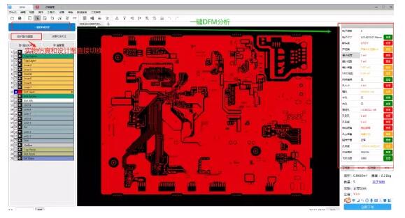
On the right is a general result of its analysis. You can click to view the detailed content to help us judge whether there is a real problem.
3. It can directly import PCB source files or Gerber files for analysis, that is to say, it is not necessary to import Gerber files for analysis every time. You can import PCB source files, including Allegro, Pads, AD and other common software.
4. You can export Gerber files, coordinate files, and screen printing pdf files with one click.
Company Tel: +86-0755-83044319
Fax/fax:+86-0755-83975897
Email: 1615456225@qq.com
QQ: 3518641314 Manager Li
QQ: 332496225 Manager Qiu
Address: Room 809, Block C, Zhantao Technology Building, No.1079 Minzhi Avenue, Longhua New District, Shenzhen



Site Map | 萨科微 | 金航标 | Slkor | Kinghelm
RU | FR | DE | IT | ES | PT | JA | KO | AR | TR | TH | MS | VI | MG | FA | ZH-TW | HR | BG | SD| GD | SN | SM | PS | LB | KY | KU | HAW | CO | AM | UZ | TG | SU | ST | ML | KK | NY | ZU | YO | TE | TA | SO| PA| NE | MN | MI | LA | LO | KM | KN
| JW | IG | HMN | HA | EO | CEB | BS | BN | UR | HT | KA | EU | AZ | HY | YI |MK | IS | BE | CY | GA | SW | SV | AF | FA | TR | TH | MT | HU | GL | ET | NL | DA | CS | FI | EL | HI | NO | PL | RO | CA | TL | IW | LV | ID | LT | SR | SQ | SL | UK
Copyright ©2015-2025 Shenzhen Slkor Micro Semicon Co., Ltd