Service hotline
+86 0755-83044319
release time:2022-03-17Author source:SlkorBrowse:11470
In the past two years, gallium nitride has developed rapidly in the field of consumer power supply. Whether it is a high-frequency QR flyback topology with high cost performance, an active clamp flyback with high performance, or an LLC dedicated to 100 watts of high power, new gallium nitride fast charging products are constantly emerging in the market.
Of course, the maturity of technology will also make the performance and selling point of products face the problem of homogenization. In order to seek more product differentiation, power supply manufacturers are also racking their brains. For example, recently, the charging head network got a new 65W gallium nitride fast charging product introduced by Armor. Besides the advantages of the current mainstream gallium nitride charger, such as small and portable, high power output and multi-device support, it also added the wireless intelligent interconnection function. Users can connect the charger through the APP, check and set the parameters of the charger, and let the charger enter the intelligent era.
Not long ago, the charging head network has also evaluated the performance and basic functions of this charger, Armor. Today, I will continue to share its disassembly with you. Let's take a look at how this charger, which can be connected to APP, is designed internally. Previously, the charging head network also dismantled an armored 20W PD fast charging charger.
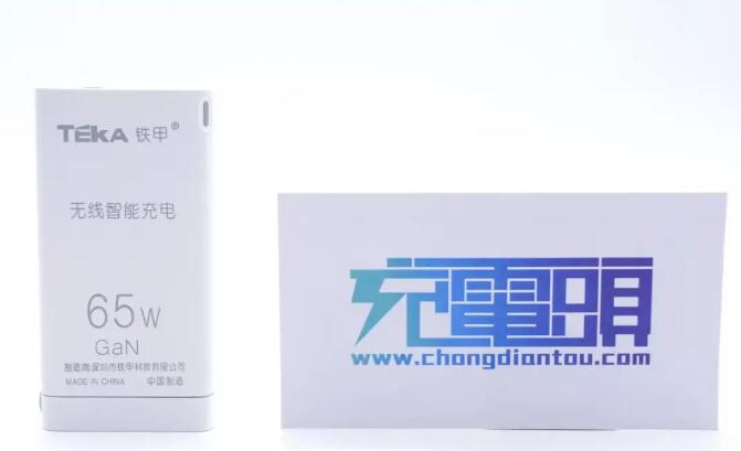
Tiejia's 65W GaN wireless intelligent charger is made of white flame retardant material, and the front side is printed with a wealth of product information, among which 65W, GaN and wireless intelligent charging are the main features of this product. Manufacturer: Shenzhen Tiejia Technology Co., Ltd.
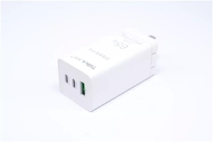
The standard output of the charger is 2C1A three output interfaces, of which two C ports can achieve 65W power when single port outputs, and can charge three devices at the same time.
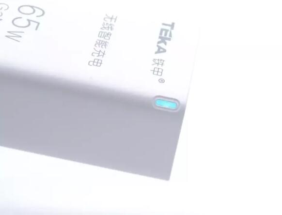
There is an LED indicator in the corner near the output end, which emits light blue light when the power is turned on.
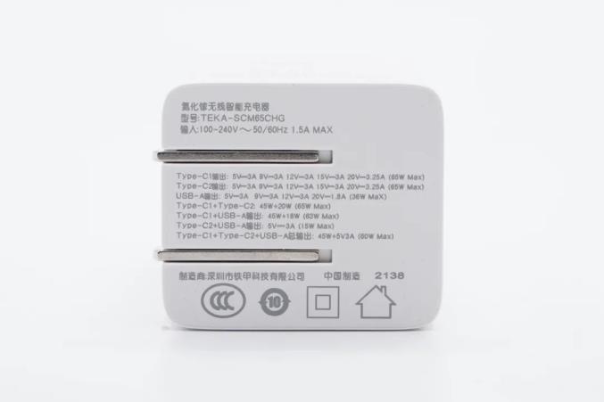
The charger is equipped with folding pins, which is convenient for storage and carrying. Specific parameter information is printed on the side of the pin, and the model is TEKA-SCM65CHG, which supports a wide voltage input of 100-240V, and the C1 interface and C2 interface both support a 65W output; A port supports 36W output at maximum; C1+C2 output: 45W+20W;; C1+A port output: 45W+18W;; C2+A output: 5V3A, C1+C2+A port output: 45W+15W.
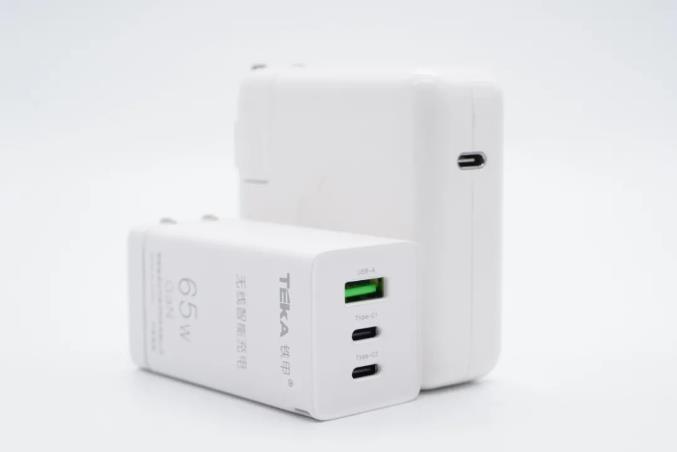
Through comparison, it is found that the volume of this 65W three-port gallium nitride fast charge of Tiejia is only about half that of Apple's original 61W fast charge.

In terms of size, the length of the charger measured by caliper is about 69.89mm.

The width is about 31.15mm .

Thickness is about 35.60mm .
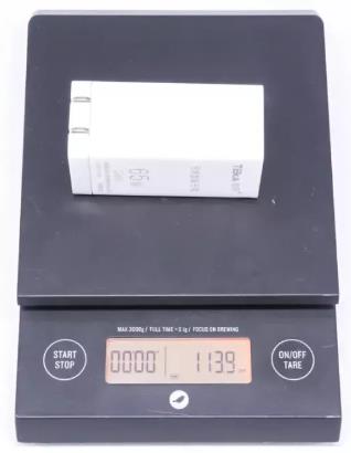
The net weight is about 113.9g .
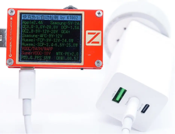
Use ChargerLAB's POWER-Z KT002 to read the fast charging protocol of USB-C1 interface, and it supports PD, PPS, Apple2.4A, QC2.0, QC3.0, QC4+, AFC, FCP, SCP and PE fast charging protocols.
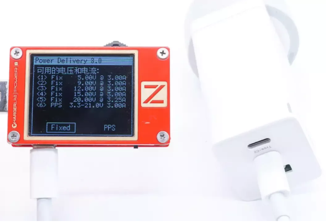
When USB-C1 triggers PD fast charging output, it can provide five fixed output gears of 5-15V3A and 20V3.25A, and a group of PPS gears of 3.3-21V3A
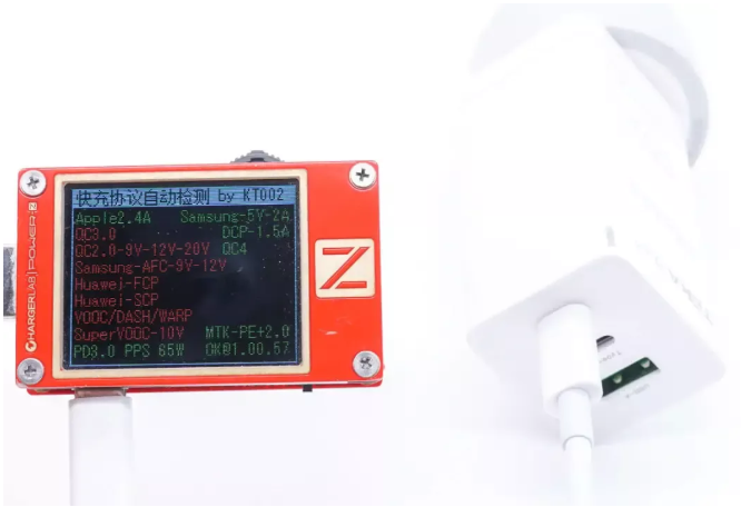
In the same way, read the fast charging protocol of USB-C2 interface, and the measured data support PD, PPS, Apple2.4A, QC4.0 and PE fast charging protocol.
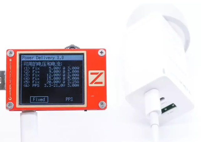
The USB-C2 also supports five fixed output gears of 5-15V3A and 20V3.25A, and a group of PPS gears of 3.3-21V3A
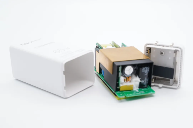
Turn on the charger and take out the internal PCB. It can be seen that its internal power module is wrapped by insulation board and brass heat sink.
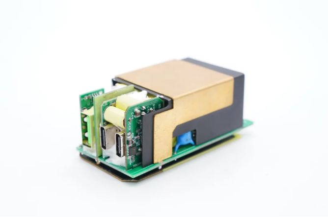
The heat sink mainly covers the AC-DC power supply part of the power module.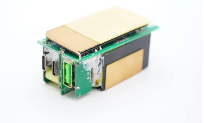
The back of the main PCB board is also covered by a heat sink.
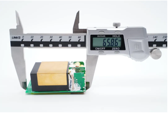
The length of the internal PCB is about 65.86mm .
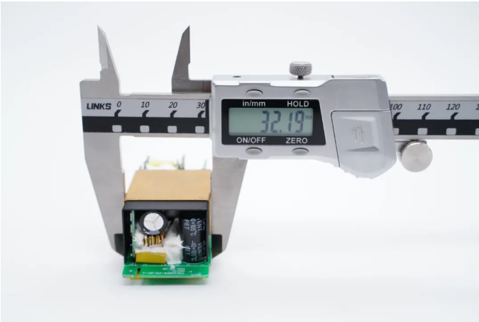
The width is about 32.19mm .
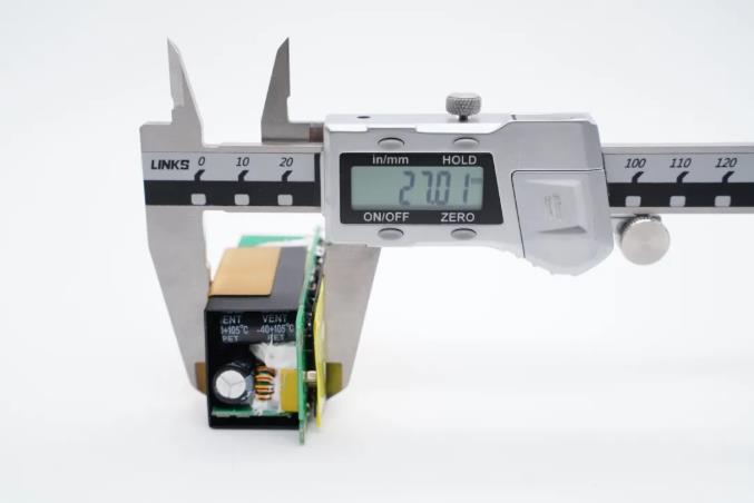
Thickness is about 27.01mm.
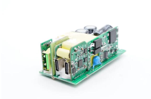
Remove the heat sink wrapped around the PCB. It can be seen that this power supply module is composed of several PCB boards, one PCB board is arranged at the side of the primary part, three interfaces at the output end are welded by one PCB board respectively, and another PCB board is used for wireless intelligent control.
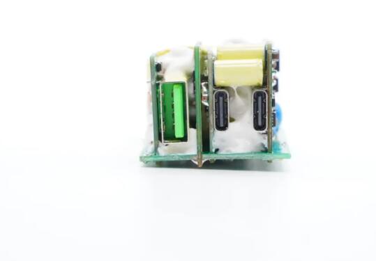
The PCB boards at the output end are treated with glue injection, which plays a role in fixing and radiating heat.
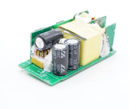
From the input side, there are mainly electrolytic capacitors, common mode choke, transformers and other devices, as well as glue injection treatment.
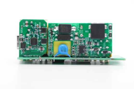
From the side, the primary PCB on the right is equipped with rectifier bridge, PWM main control chip, Y capacitor, optocoupler and other devices, while the PCB on the left is equipped with secondary step-down circuit.
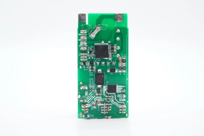
The back of PCB is equipped with gallium nitride chip, Y capacitor, synchronous rectification MOS and other devices.
According to the observation and analysis of the charging head network, this power supply module outputs a fixed voltage from the switching power supply, and then realizes multi-port fast charging output through the secondary step-down circuit. Among them, the switching power supply part adopts the industry mainstream high-frequency QR flyback topology structure, and the secondary part has an Internet of Things module independently besides the conventional secondary step-down circuit.
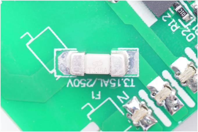
A 3.15A delay fuse is used at the input.
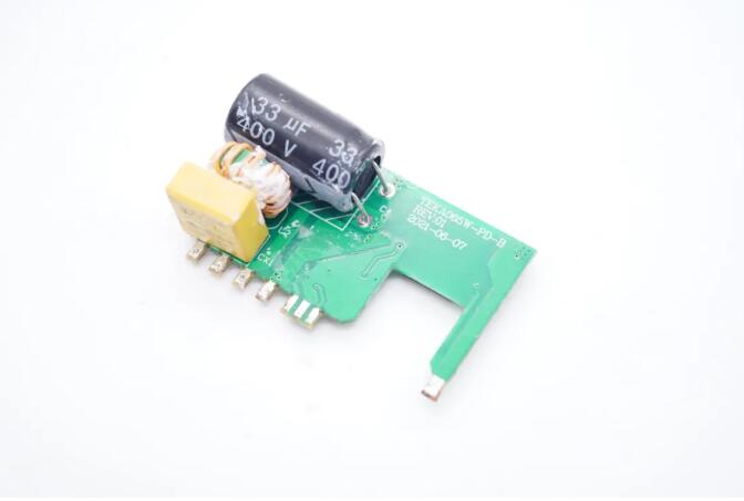
将侧面PCB板拆除,上面设有一颗共模电感、一颗安规X电容和一颗高压滤波电解电容。
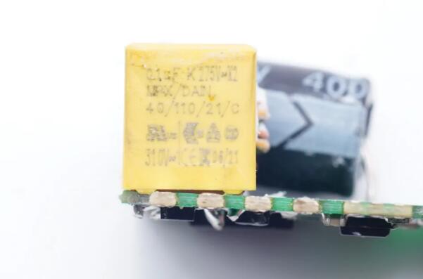
The specification of ampere X2 capacitor is 0.1 μ f.
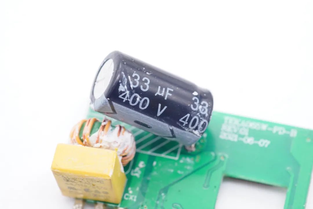
The electrolytic capacitor of high voltage filter is 400V 33μF .
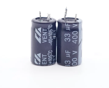
In addition, two high-voltage electrolytic capacitors are located on the main PCB board, and their specifications are 400V 33μF f.
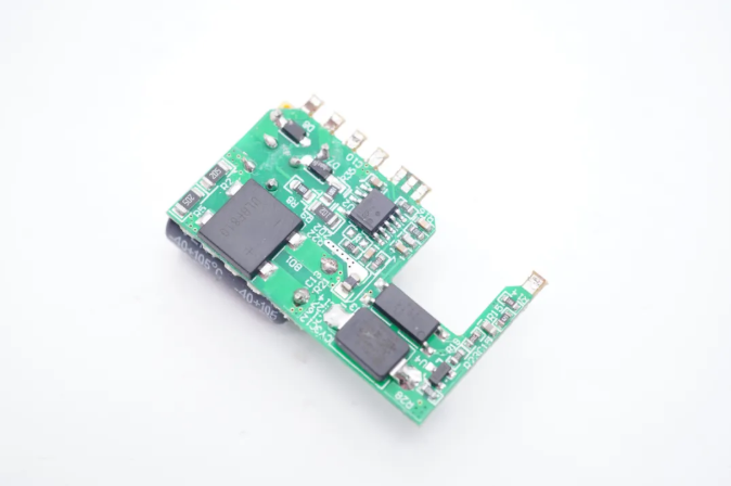
Let's take a look at the main devices on the back of PCB.
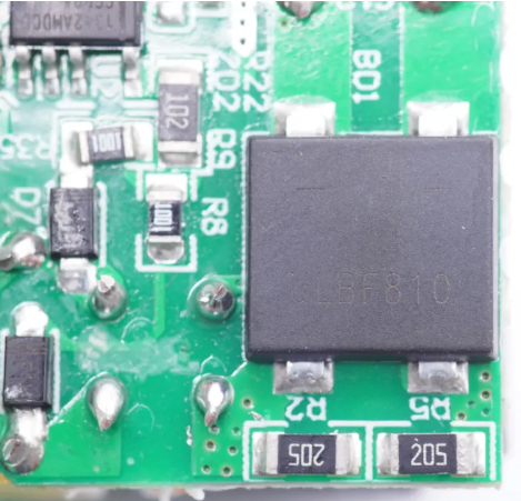
Printed rectifier bridge of LBF810.
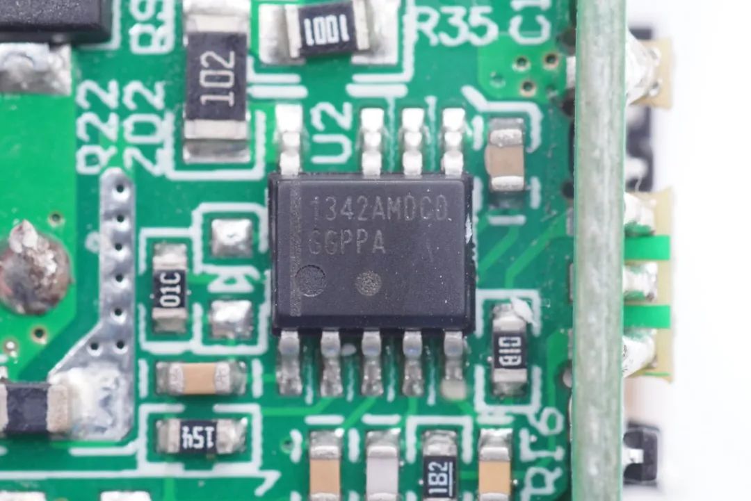
The main control chip of gallium nitride is Ansanmei NCP1342. It is a high-frequency flyback quasi-resonant primary PWM controller with built-in active X2 capacitor discharge, wide range Vcc power supply, external thermistor for overheating protection and multiple perfect protection functions.
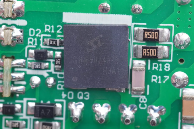
The gallium nitride switch tube model of the charger is G1N65R240PB, which comes from Zhuhai Gallium Future Technology Co., Ltd. The device is packaged in PQFN8*8, with a withstand voltage of 650V, a transimpedance of 240mΩ, and a gate withstand voltage of ± 18V, without negative voltage driving, simplifying the driver design. It is suitable for high-frequency compact QR or ACF flyback architecture, half-bridge buck/boost, totem pole PFC circuit or inverter circuit, high-frequency efficient LLC or other soft-switching topologies.
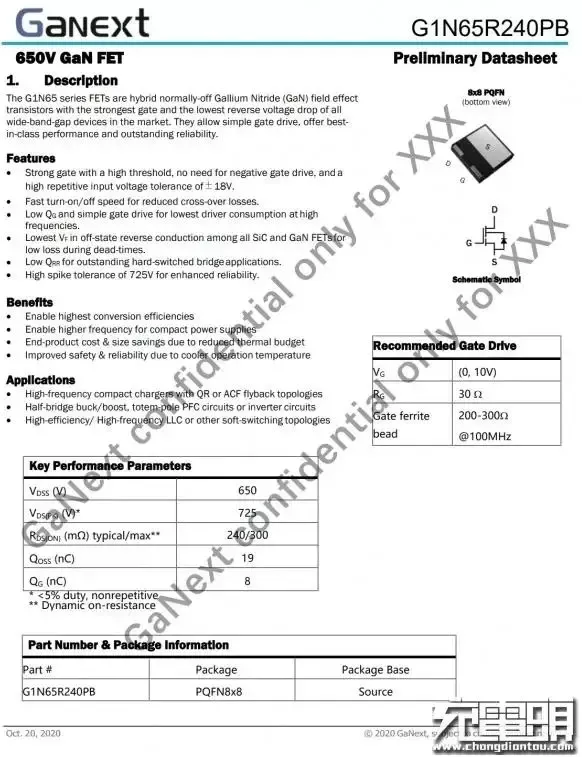
According to the charging network, this gallium nitride power device has been previously adopted by products such as Green Giant Energy 65W three-port gallium nitride fast charging charger, Yuemi 65W 1A1C gallium nitride fast charging charger, Weiwofeng 65W 2C1A gallium nitride fast charging charger, etc.
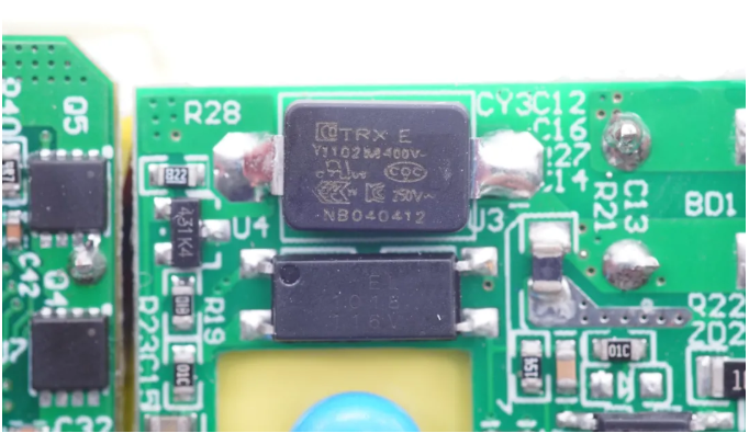
Chip Y capacitor is from Teruixiang from Sichuan Teruixiang Technology Co., Ltd., which has the characteristics of small size and light weight, and is very suitable for high-density power products such as gallium nitride fast charging.
Ruixiang focuses on R&D, production and sales of passive components with a registered capital of 100 million yuan. There are two kinds of independent capacitor brands: SMD TRX and DIP TY capacitors. TRX will devote itself to the research of ceramic materials to expand the application of more categories and provide more solutions for customers.
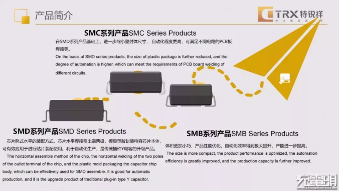
According to the charging network, Teruixiang SMD Y capacitor is not only used by dozens of fast charging products of brands such as Belgin, Anke, QCY, Shengli, Maiduoduo, OPPO, Lenovo, Nubia, Beisi, Hailutong, Daiwei, but also used by Igor 40W LED driving power supply, Changhong 42-inch intelligent network TV 42P3F built-in power supply, Zhuofeihang 45W gallium nitride ultra-fast wall charging and other products.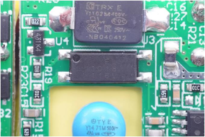
The light coupler comes from EL Yiguang and is used for output voltage feedback.
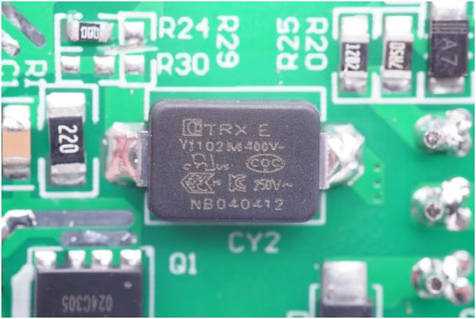
The main PCB board is also equipped with a special Y capacitor.
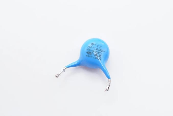
There is also a plug-in Y capacitor.
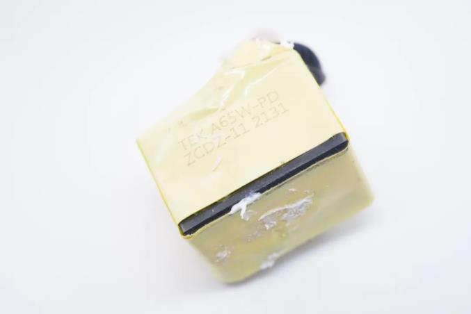
The transformer is wrapped with insulating tape, and information such as power is silk-printed.
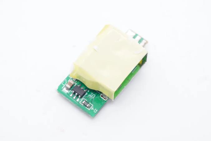
The rectifier chip is set on the PCB where USB-A interface is located. Except synchronous rectification controller, there is no other control circuit on PCB.
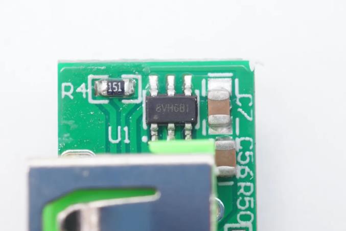
This synchronous rectification controller is from Xinmaowei, model LP35118V, and is packaged in SOT23-6L, which is suitable for isolated switching power supply applications. Support forward and flyback topologies, DCM and CCM working modes. With ultra-fast turn-off speed, it can reduce the switching loss in CCM mode. At the same time, LP35118V also has built-in VCC power supply technology to ensure that it can work normally under different outputs without auxiliary power supply.
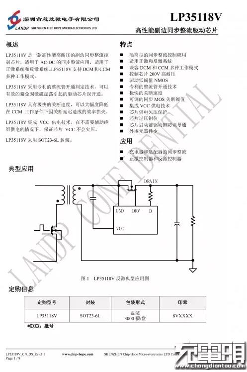
Maowei LP35118V has a maximum withstand voltage of 200V, can use logic voltage driven NMOS, has built-in proprietary rectifier bridge conduction technology, and has ultra-fast turn-off speed and adjustable synchronous rectifier turn-off threshold. Built-in VCC undervoltage protection, overvoltage clamping, driving noise suppression and other functions, simplified peripheral components, and synchronous rectification for chargers and adapters.
According to Tou.com, the products using this chip include Jiletang 20W 1A1C fast charging charger, Yuemi 65W 1A1C gallium nitride fast charging charger, Weiwofeng 65W21A gallium nitride fast charging charger, etc.
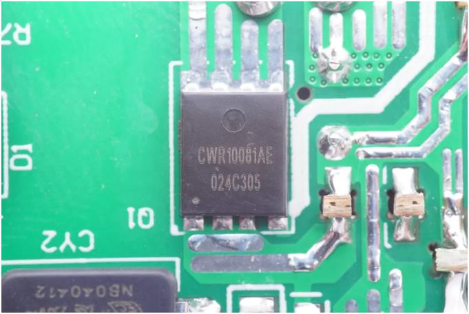
Synchronous rectification MOS screen printing CWR10081AE.

The synchronous rectification output filter adopts a 10-megapixel solid-state capacitor with a specification of 25V 470μF, which is insulated by winding tape.
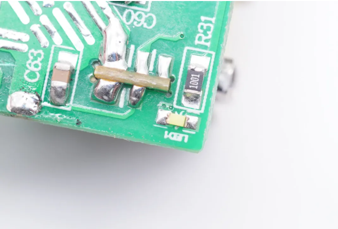
The corner of the main PCB board is provided with an LED indicator.
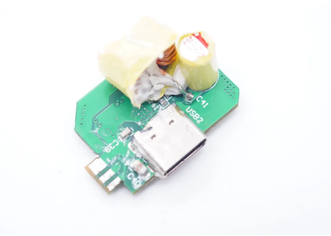
Remove the PCB where the C2 interface is located, and the front side is provided with a step-down inductor, a filter capacitor and a USB-C interface.
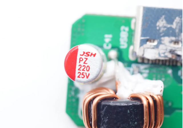
The output filter uses a 25V 220μF solid-state capacitor from Wanjingyuan.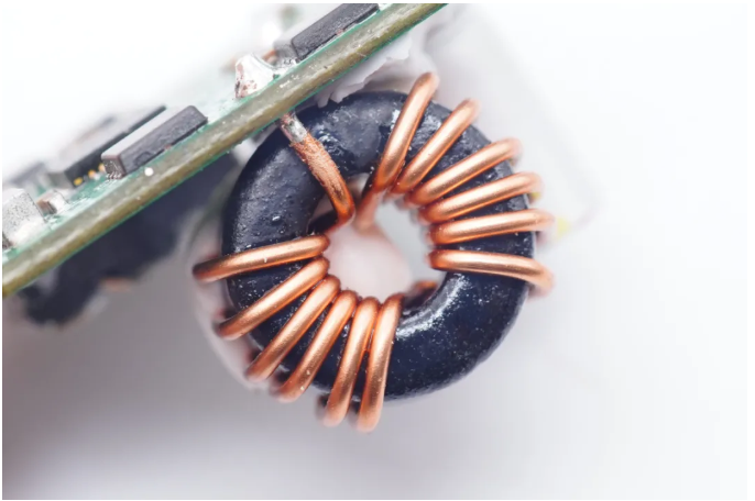
Close-up of step-down inductor.
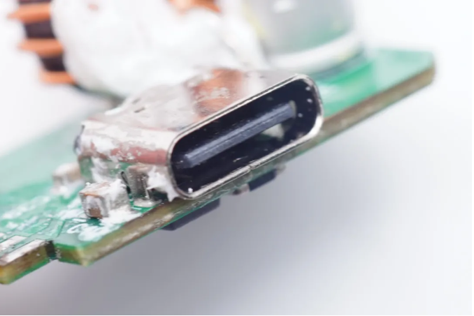
Close-up of C2 interface.
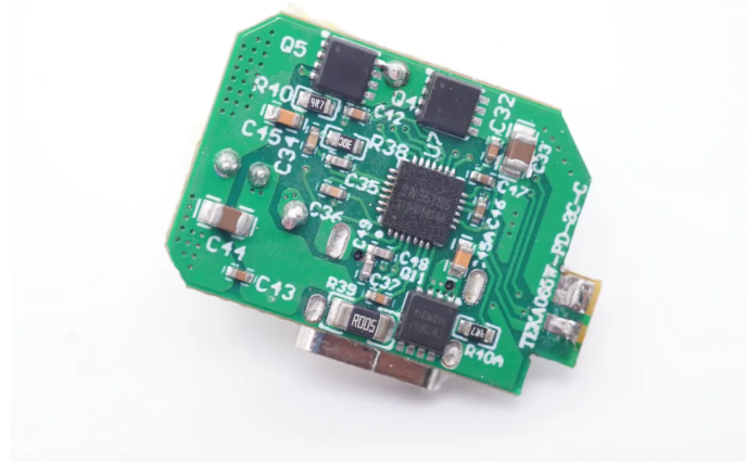
At the center of the back of the PCB is a highly integrated buck controller, two buck MOS tubes, and a VBUS switch tube.
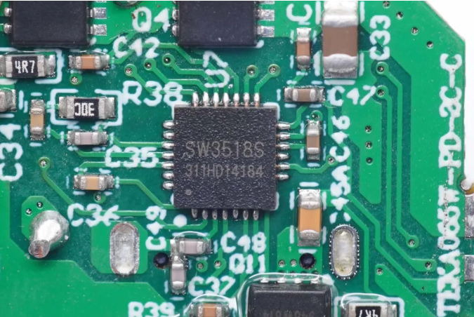
SW3518S, a highly integrated step-down and protocol identification chip from Zhirong, is a highly integrated dual-port charging chip with multiple fast charging protocols, and has passed the VOOC certification. The chip supports arbitrary fast charging output of A+C port, supports independent current limiting of two ports, integrates 5A high-efficiency synchronous buck converter, and supports PPS, PD, QC, AFC, FCP, SCP, PE, SFCP, VOOC and other fast charging protocols, with a maximum output of PD100W.
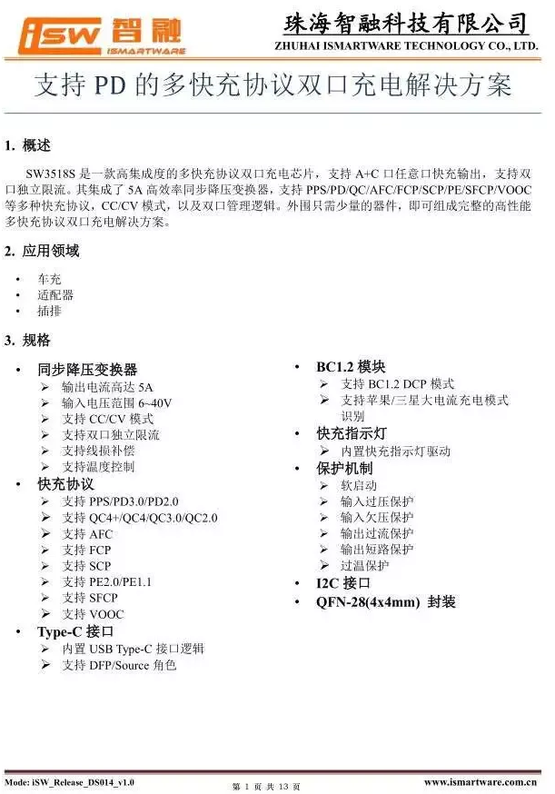
According to the dismantling of the charging network, Zhirong SW3518S has been quickly charged by Elsa Watt 65W21C gallium nitride, flash 90W21A gallium nitride, Philips 65W gallium nitride fast charging socket, Lei Bai 65W GaN fast charging, Dianyou 65W21A gallium nitride fast charging, etc. In addition, Zhirong's fast charging chip can also be used in USB PD fast charging mobile power supply, fast charging car charging and other fields.
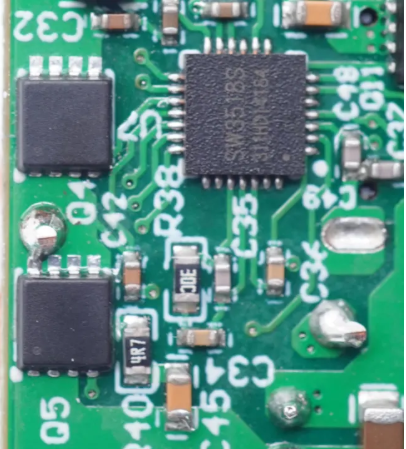
Two external buck MOS tubes have no screen printing information.
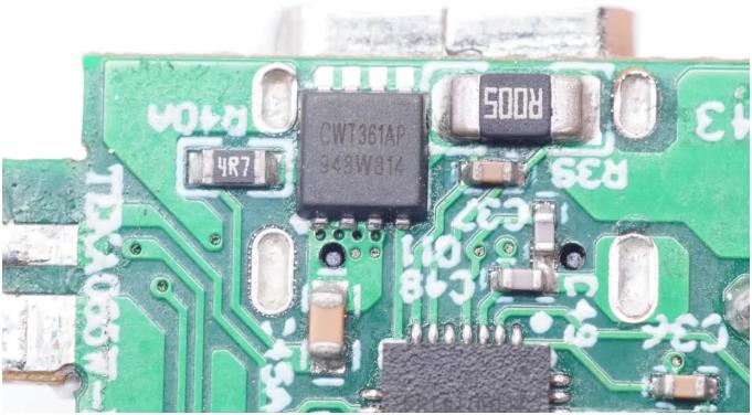
Screen printing of VBUS switch tube CWT361AP.
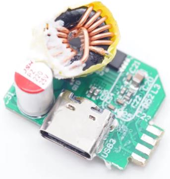
The front of the PCB where the interface C1 is located is provided with a step-down inductor, capacitor, interface, and MOS.
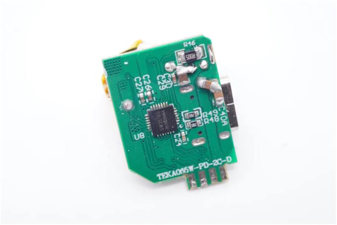
There is a main control chip on the back.
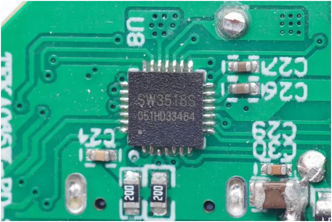
The main control chip also uses Zhirong SW3518S.
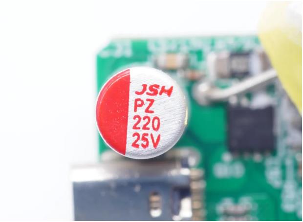
Output filtered solid-state capacitor from Wanjingyuan.
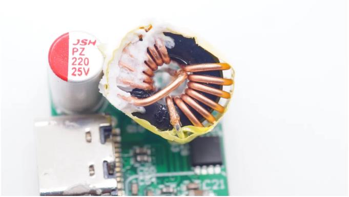
Close-up of step-down inductor.
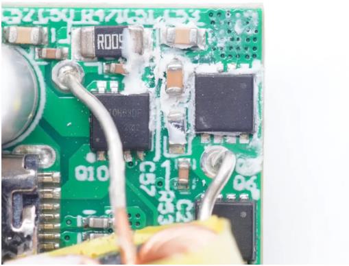
Below the buck inductor are three MOS tubes, two of which are used at the edge to configure Smart SW3518S for buck, and the other is used as VBUS switch tube.
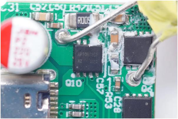
Output VBUS switch tube screen printing AP10H03DF.
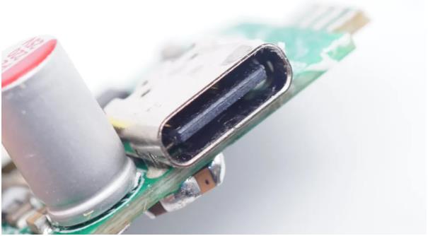
C1输出接口特写。Close-up of C1 output interface.
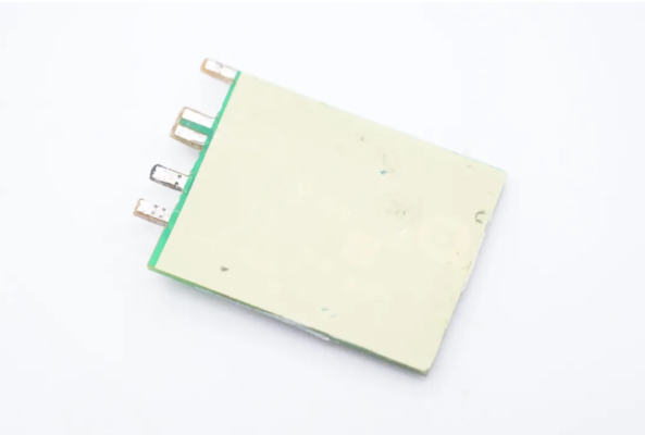
Then look at the wireless intelligent control PCB module, one side of which has no components and is insulated with insulating tape.
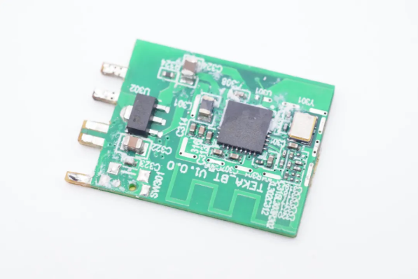
In addition, there is a main control chip, LDO and crystal oscillator. In addition, there is a printed antenna on the PCB with the words TKEA_BT printed by silk screen.
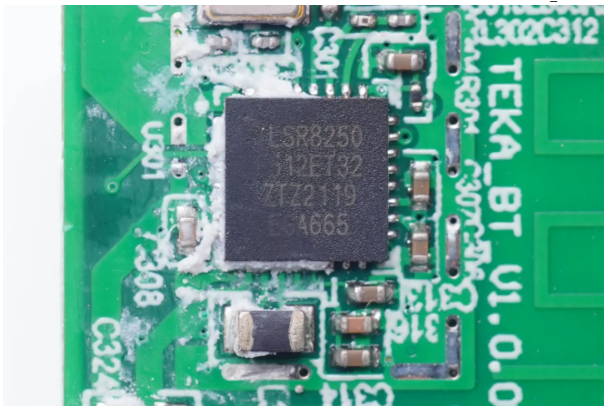
Printed Bluetooth chip of LSR8250.
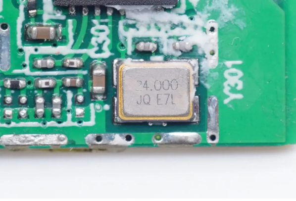
External 24.000MHz passive crystal oscillator.
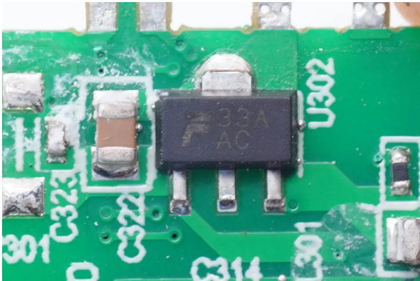
LDO for supplying power to the main control chip.
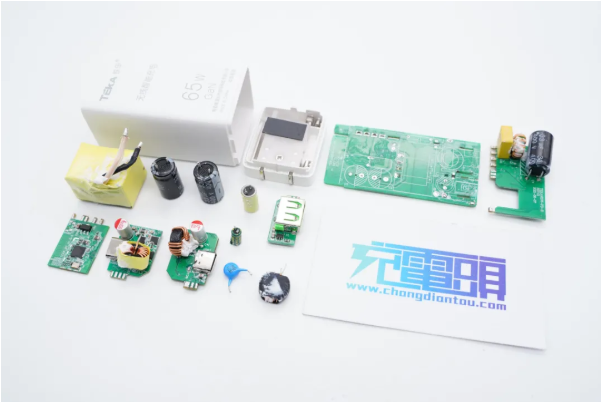
Iron 65W gallium nitride fast charging charger is completely disassembled.
In terms of appearance, the fast charging of 65W gallium nitride in Armor is similar to the common gallium nitride fast charging products on the market. It has a long body, three interfaces with folding pins and 2C1A, and a status indicator. Compared with the fast charging of traditional power devices, its volume is much smaller. The performance is also at the mainstream level in the industry, which is compatible with many mainstream fast charging protocols on the market, and supports dual C-port blind plug-in output of 65W and multi-port power intelligent distribution function.
The biggest feature of this charger is the addition of Bluetooth wireless connection function. Users can control it through APP, and it is very convenient to realize power distribution, output power, power cut-off, control indicator lights and so on on on the mobile phone.
According to the dismantling of the charging head network, the charger of Tiejia is based on the industry mainstream switching power supply+secondary step-down architecture design. NCP1342+ gallium future GaN devices are used in the switching power supply, and Xinmao micro-synchronous rectifier controller is selected. The outputs of the three interfaces are composed of two secondary step-down circuits, all controlled by Zhirong SW3518S; In addition, a Bluetooth module is added to realize the intelligent connection and output control between the charger and the mobile APP.
Disclaimer: This article is reproduced from "Charging Head Network". This article only represents the author's personal views, and does not represent the views of Sacco Micro and the industry. It is only for reprinting and sharing to support the protection of intellectual property rights. Please indicate the original source and author when reprinting. If there is any infringement, please contact us to delete it.
Company Tel: +86-0755-83044319
Fax/fax:+86-0755-83975897
Email: 1615456225@qq.com
QQ: 332496225 Manager Qiu
Address: Room 809, Block C, Zhantao Technology Building, No.1079 Minzhi Avenue, Longhua New District, Shenzhen



Site Map | 萨科微 | 金航标 | Slkor | Kinghelm
RU | FR | DE | IT | ES | PT | JA | KO | AR | TR | TH | MS | VI | MG | FA | ZH-TW | HR | BG | SD| GD | SN | SM | PS | LB | KY | KU | HAW | CO | AM | UZ | TG | SU | ST | ML | KK | NY | ZU | YO | TE | TA | SO| PA| NE | MN | MI | LA | LO | KM | KN
| JW | IG | HMN | HA | EO | CEB | BS | BN | UR | HT | KA | EU | AZ | HY | YI |MK | IS | BE | CY | GA | SW | SV | AF | FA | TR | TH | MT | HU | GL | ET | NL | DA | CS | FI | EL | HI | NO | PL | RO | CA | TL | IW | LV | ID | LT | SR | SQ | SL | UK
Copyright ©2015-2025 Shenzhen Slkor Micro Semicon Co., Ltd