Service hotline
+86 0755-83044319
release time:2024-12-23Author source:SlkorBrowse:8027
In the daily operation of electronic devices, transient voltage suppression is a critical task. To effectively address the overvoltage transients that may occur in circuits, the Transient Voltage Suppressor (TVS) diode was developed. Among them, the SBJ12A stands out as a high-performance transient voltage suppressor diode, with its excellent electrical characteristics and stability, making it a preferred choice in various applications.
The SBJ12A adopts a unidirectional polarity design, meaning it is specifically optimized for one-way current protection. In a circuit, it ensures that current flows only in one direction, effectively preventing the potential threat posed by reverse current. This design gives the SBJ12A a unique advantage in circuits requiring unidirectional protection, such as power input terminals and signal lines.
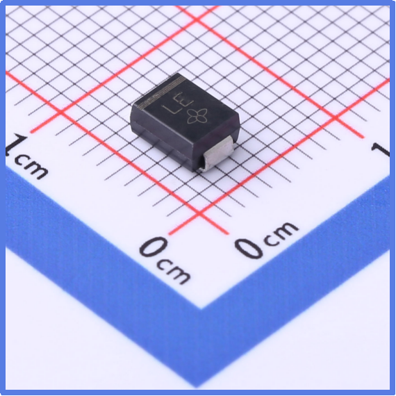
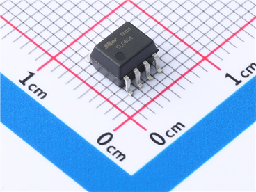
Slkor Transient Protection Diode SBJ12A product photo
The SBJ12A’s reverse working voltage (Vrwm) is 12V, which means that under normal operating voltage, the diode remains in the off state with no impact on the circuit. When the voltage exceeds this threshold, the diode will quickly conduct to dissipate the overvoltage energy. Its breakdown voltage range is between 13.3V and 15.3V. This precisely controlled breakdown voltage range allows the SBJ12A to provide accurate protection in circuits with different voltage levels.
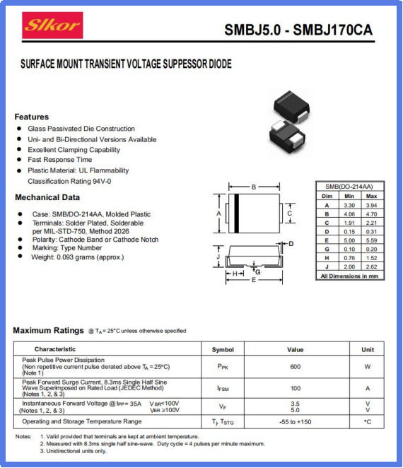
Slkor Transient Protection Diode SBJ12A specification
Reverse leakage current (Ir) is an important indicator for measuring how much current leaks through the diode when it is in the off state. The SBJ12A has a reverse leakage current of just 5μA, ensuring that the diode consumes almost no energy in its off state, thus improving the overall energy efficiency of the circuit.
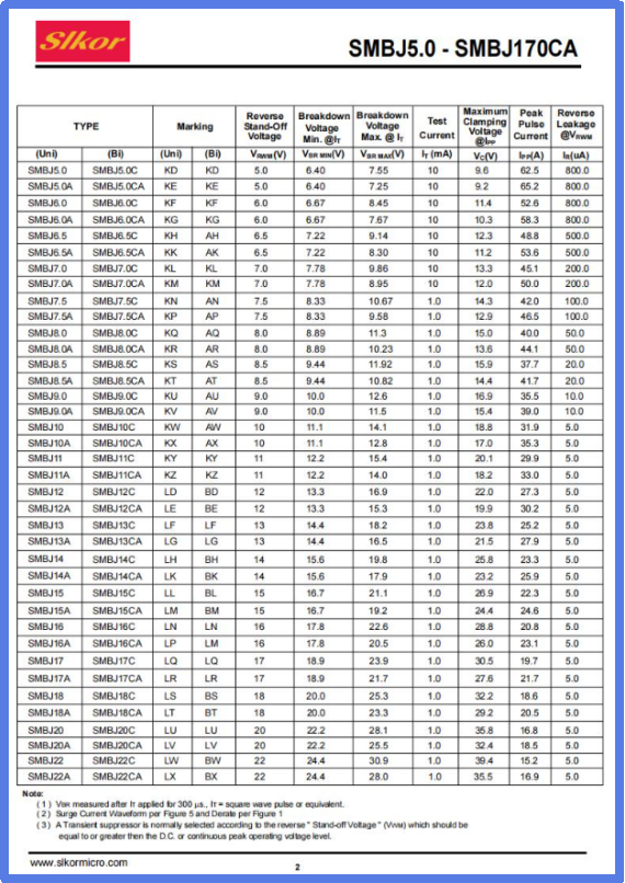
Parameters of Slkor Transient Protection Diode SBJ12A
In the face of transient overvoltage that may occur in circuits, the SBJ12A demonstrates impressive endurance. Its peak pulse current (Ipp) reaches 30.2A under the 10/1000μs waveform, meaning that even under intense transient surges, the SBJ12A can respond quickly, dissipating the overvoltage energy effectively and protecting the circuit from damage.
During the dissipation of transient overvoltage, the voltage across the diode rises rapidly. The SBJ12A’s maximum clamping voltage is 19.9V, ensuring that even under the harshest conditions, the voltage across the diode will not exceed this safety threshold, thereby effectively protecting other components in the circuit from overvoltage damage.
Peak pulse power (Ppp) is a key indicator of a diode's ability to withstand power during transient events. The SBJ12A demonstrates excellent peak pulse power performance under the 10/1000μs waveform, fully showcasing its strong reliability and performance when dealing with transient overvoltage.
During the process of dissipating overvoltage, the voltage across the diode rises rapidly. The maximum clamping voltage, as the name suggests, is the highest voltage the diode will reach during this dissipation process. This value is crucial for protecting other components in the circuit.
Limiting Voltage Rise: When overvoltage occurs, the transient voltage suppressor diode will quickly conduct and dissipate the overvoltage energy through its internal PN junction structure. During this process, the voltage across the diode rises, but the maximum clamping voltage limits the extent of the rise, ensuring the voltage does not exceed a safe threshold.
Protecting Other Components: Other components in the circuit, such as transistors and integrated circuits, have their own maximum operating voltage limits. If the voltage across the diode exceeds the maximum operating voltage of these components due to transient overvoltage, they may be damaged. The maximum clamping voltage ensures that the voltage across the diode does not surpass this safety threshold, thus protecting other components in the circuit.
Improving Circuit Reliability: By limiting the voltage rise and protecting other components, the maximum clamping voltage indirectly enhances the overall reliability of the circuit. It ensures that the circuit can operate more stably when faced with transient overvoltage, reducing failures and damage caused by overvoltage.
Slkor has research and development offices in Busan, South Korea, Beijing, China, and Suzhou, China. Most of the wafer manufacturing and packaging and testing are carried out within China. The company employs and collaborates with individuals and organizations worldwide, with a laboratory for product performance and reliability testing and a central warehouse located at its headquarters in Shenzhen. Slkor has filed for over a hundred invention patents, offers more than 2,000 product models, and serves over ten thousand customers globally. Its products are exported to countries and regions including Europe, the Americas, Southeast Asia, and the Middle East, making it one of the rapidly growing semiconductor companies in recent years. With well-established management systems and streamlined workflows, Slkor has rapidly enhanced the brand awareness and reputation of its "SLKOR" brand through its outstanding quality and standardized services. Its product range includes three major series: diodes, transistors, and power devices, with recent introductions of new products such as Hall elements and analog devices, expanding its presence in sensors, Risc-v microcontrollers, and other product categories.



Site Map | 萨科微 | 金航标 | Slkor | Kinghelm
RU | FR | DE | IT | ES | PT | JA | KO | AR | TR | TH | MS | VI | MG | FA | ZH-TW | HR | BG | SD| GD | SN | SM | PS | LB | KY | KU | HAW | CO | AM | UZ | TG | SU | ST | ML | KK | NY | ZU | YO | TE | TA | SO| PA| NE | MN | MI | LA | LO | KM | KN
| JW | IG | HMN | HA | EO | CEB | BS | BN | UR | HT | KA | EU | AZ | HY | YI |MK | IS | BE | CY | GA | SW | SV | AF | FA | TR | TH | MT | HU | GL | ET | NL | DA | CS | FI | EL | HI | NO | PL | RO | CA | TL | IW | LV | ID | LT | SR | SQ | SL | UK
Copyright ©2015-2025 Shenzhen Slkor Micro Semicon Co., Ltd