Service hotline
+86 0755-83044319
release time:2022-03-17Author source:SlkorBrowse:10558
It is said that in 2018 AD, the heads of the sixth and seventh generations of IGBT rivers and lakes were surprised, and there was no difference in the limelight for a while. People from all walks of life who ate melons speculated on the origins of the two heroes. Can't help but have a good Samaritan combed the British family over the years, and the leading generations of leaders are:

Well, I can't seem to tell who's here.

Er, although these IGBT "heads" all look the same on the surface, they are all man show-type. I can only take off my clothes and have a "core" dirty operation. . .
Like this, on the chip, cut it sideways.
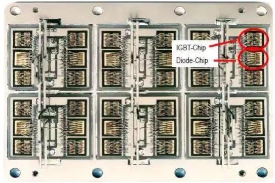
It seems, it's a little different. . .
Let's start the story here. . .

Prehistoric times -PT
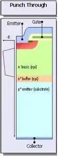
PT is the first generation IGBT, which uses heavily doped P+ substrate as the starting layer, on which N+ buffer and N- base epitaxy are grown in turn, and finally a cellular structure is formed on the surface of the epitaxial layer. It is named because the electric field runs through the whole N-base area when it is cut off. It has complex process, high cost, and needs carrier life control. The saturation voltage drop has a negative temperature coefficient, which is not conducive to parallel connection. Although it was once a storm in the 1980s, it was gradually replaced by NPT in the late 1980s, and now it has become a recluse. At present, all IGBT products of Infineon do not use PT technology.
First generation leader -IGBT2
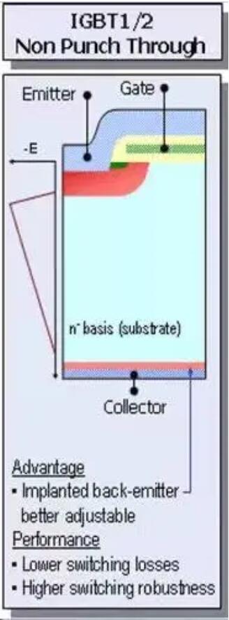
Features:Gate, non-punch-through structure (NPT)
NPT-IGBT came out of the mountain in 1987, and soon became the dominant player in the 1990s. Unlike NPT PT, it uses a low-doped N- substrate as the starting layer, first makes a MOS structure on the front side of the N- drift region, then thins it from the back side to the thickness required by IGBT voltage specification by grinding and thinning process, and then forms a P+ collector from the back side by ion implantation process. The electric field does not penetrate through the N- drift region at the turn-off, so it is called "non-punch-through" IGBT. NPT doesn't need carrier lifetime control, but its disadvantage is that if it needs higher voltage blocking capability, it will inevitably need a higher resistivity and thicker N- drift layer, which means that the saturated conduction voltage Vce(sat) will also rise, thus greatly increasing the loss and temperature rise of the device.
Skills:Keywords low saturation pressure drop, positive temperature coefficient,15℃ junction temperature, high robustness.
Because the thickness of N- drift region is greatly reduced, Vce(sat) is greatly reduced compared with PT. Positive temperature coefficient is favorable for parallel connection.
name:
DLC,KF2C,S4…
Wait, something strange seems to have been mixed in!That's right!
S4 is really not IGBT4, it is IGBT2 with bright red roots, which is suitable for high-frequency switching applications, and the hard switching frequency can reach 40kHz. This star product still sells well up to now.
Performance leap -IGBT3
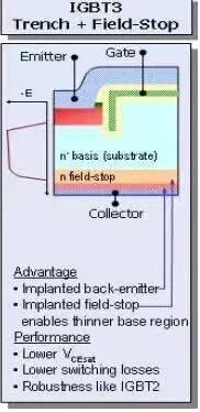
Features:Gate, Field Stop
The appearance of IGBT3 has brought about a great change in IGBT. The cell structure of IGBT3 changed from planar to trench. In the trench IGBT, the electron channel is perpendicular to the surface of the silicon wafer, which eliminates the JFET structure, increases the surface channel density and near-surface carrier concentration, thus making the performance more optimized. If you want to know more about the difference between planar gate and trench gate technology, you can refer to our previously published article "Analysis of planar and trench IGBT structures".
In terms of vertical structure, in order to alleviate the contradiction between blocking voltage and saturation voltage drop, the British company introduced Field Stop IGBT in 2000, with the aim of minimizing the thickness of drift region, thus reducing saturation voltage. The starting material of Field Stop)IGBT is the same as NPT, which is a low doped N- substrate. The difference is that an additional N- buffer layer is injected into the back of FS IGBT, and its doping concentration is slightly higher than that of N- substrate. Therefore, it can quickly reduce the electric field intensity and make the whole electric field trapezoidal, thus greatly reducing the thickness of the required N-drift region. In addition, N buffer can also reduce the emission efficiency of p emitter, thus reducing the tail current and loss when it is turned off. If you want to know more about the difference between NPT and field stop devices, please go to "Differences of PT, NPT and FS IGBT" for more details.
Skills:Low conduction voltage drop,25℃ working junction temperature,Switch performance optimization
Thanks to the field cut-off and trench cell, the on-state voltage drop of IGBT3 is lower, and the typical Vce(sat) ranges from 3.4 in the second generation to 2.55 V in the third generation (3300 V for example).
name:
T3,E3,L3
IGBT3 has basically been replaced by IGBT4 in the medium and low voltage field, but it still dominates in the high voltage field. For example, the mainstream products of 3300V, 4500V and 6500V still use IGBT3 technology.
中流砥柱-IGBT4
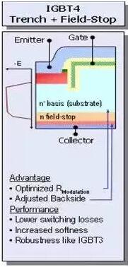
IGBT4是目前使用最广泛的IGBT芯片技术,电压包含600V,1200V,1700V,电流从10A到3600A,各种应用中都可以见到它的身影。
Features:Gate+field cut-off+thin wafer
Like IGBT3, it has the structure of field cut-off and trench gate, but IGBT4 optimizes the back structure, the drift region is thinner, and the doping concentration and emission efficiency of P emitter and N buffer on the back are optimized.
Skills:High switching frequency,Optimize switch softness,Operating junction temperature of 50℃
By using thin wafers and optimizing the back structure of IGBT4, the switching loss is further reduced, and the switching softness is higher. At the same time, the maximum allowable junction temperature is increased from 125℃ of the third generation to 150℃, which will undoubtedly further increase the output current capability of the device.
name:
T4,E4,P4
T4 is a low-power series with the highest switching frequency of 20kHz.
E4 is suitable for medium power applications, and its switching frequency is up to 8kHz.
P4' s switching softness is further optimized, which is more suitable for high-power applications. The switching frequency is up to 3kHz.
Disclaimer: This article is reproduced from "Electronic Enthusiast Network". This article only represents the author's personal views, and does not represent the views of Sacco Micro and the industry. It is only for reprinting and sharing to support the protection of intellectual property rights. Please indicate the original source and author when reprinting. If there is any infringement, please contact us to delete it.
Company Tel: +86-0755-83044319
Fax/fax:+86-0755-83975897
Email: 1615456225@qq.com
QQ: 3518641314 Manager Li
QQ: 332496225 Manager Qiu
Address: Room 809, Block C, Zhantao Technology Building, No.1079 Minzhi Avenue, Longhua New District, Shenzhen



Site Map | 萨科微 | 金航标 | Slkor | Kinghelm
RU | FR | DE | IT | ES | PT | JA | KO | AR | TR | TH | MS | VI | MG | FA | ZH-TW | HR | BG | SD| GD | SN | SM | PS | LB | KY | KU | HAW | CO | AM | UZ | TG | SU | ST | ML | KK | NY | ZU | YO | TE | TA | SO| PA| NE | MN | MI | LA | LO | KM | KN
| JW | IG | HMN | HA | EO | CEB | BS | BN | UR | HT | KA | EU | AZ | HY | YI |MK | IS | BE | CY | GA | SW | SV | AF | FA | TR | TH | MT | HU | GL | ET | NL | DA | CS | FI | EL | HI | NO | PL | RO | CA | TL | IW | LV | ID | LT | SR | SQ | SL | UK
Copyright ©2015-2025 Shenzhen Slkor Micro Semicon Co., Ltd