Service hotline
+86 0755-83044319
release time:2022-03-17Author source:SlkorBrowse:9598
1.
system definition
System definition is the basic premise of analog circuit design. According to the design requirements, analog circuit design engineers need to make corresponding functional definitions of circuit systems and subsystems, and determine the parameter ranges of area, power consumption and other related performance.
2.
circuit designThe selection of circuit structure is an important link in circuit design. Analog circuit design engineers need to select the appropriate circuit structure according to the functional requirements, design specifications and corresponding parameters of analog circuits, and on this basis, determine the combination of components. For the design of analog electronic circuits, there is no mature design software available at present, so engineers can only do it manually according to their own experience. To some extent, this increases the difficulty of analog circuit design and limits the development speed of analog circuit.
3.
Circuit simulation
Circuit simulation is an indispensable link in the design process of analog circuits, and it is an important basis for analog engineers to judge whether analog circuits can meet the design requirements.
According to the simulation results, engineers constantly modify and adjust the circuit until the simulation results of the analog circuit can meet the set indicators and corresponding functional requirements. Commonly used methods include parameter scanning, DC and AC analysis, Monte Carlo analysis, etc.
4.
Layout realization
An important bridge to transform circuit design into production. After the structure and related parameters of the analog circuit are determined by the previous design and simulation results, the design engineer describes the physical geometry of the designed analog circuit and converts it into a graphic format, so as to facilitate the subsequent processing and manufacture of the analog circuit.
5.
Physical verification
In the stage of physical verification, it is necessary to check the design rules (DRC) of the designed analog circuit. The design rule check is to check the minimum line width, hole size, minimum pattern spacing and other restricted processes based on the given design rules, so as to measure the feasibility of layout process implementation. In addition, the consistency of layout and circuit diagram should be checked (LVS). The parameters of layout can be extracted by LVS tool, and the obtained circuit diagram can be compared with the original circuit design to ensure the consistency between layout and the original circuit design.
6.
Simulation after parasitic parameter extraction
The simulation of circuit design before layout is called "pre-simulation", which is an ideal simulation without considering parasitic parameters such as resistance and capacitance of the wiring. After parasitic parameters are added to the layout, the circuit simulation is called "post-simulation". Only when the simulation results of post-simulation meet the design index and system function requirements, the circuit design is completed.
Parasitic parameters have a great influence on analog circuits. When the simulation results of the former simulation meet the requirements, the latter simulation results cannot meet the requirements. Therefore, design engineers need to constantly modify the transistor parameters according to the post-simulation results, and sometimes even adjust the circuit structure until the post-simulation results meet the system design requirements.
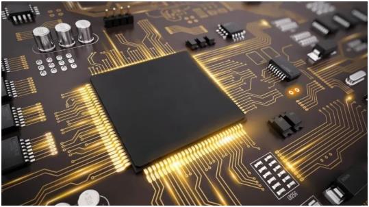
At the same time, the following eleven details should be paid attention to in analog circuit design:
 (1) In order to obtain a feedback circuit with good stability, it is usually required to use a small resistor or choke outside the feedback loop to provide a buffer for the capacitive load.
Disclaimer: This article is reproduced from "Gu Taiwei". This article only represents the author's personal views, and does not represent the views of Sacco Wei and the industry. It is only for reprinting and sharing to support the protection of intellectual property rights. Please indicate the original source and author when reprinting. If there is any infringement, please contact us to delete it.
Company Tel: +86-0755-83044319
Fax/fax:+86-0755-83975897
Email: 1615456225@qq.com
QQ: 332496225 Manager Qiu
Address: Room 809, Block C, Zhantao Technology Building, No.1079 Minzhi Avenue, Longhua New District, Shenzhen



Site Map | 萨科微 | 金航标 | Slkor | Kinghelm
RU | FR | DE | IT | ES | PT | JA | KO | AR | TR | TH | MS | VI | MG | FA | ZH-TW | HR | BG | SD| GD | SN | SM | PS | LB | KY | KU | HAW | CO | AM | UZ | TG | SU | ST | ML | KK | NY | ZU | YO | TE | TA | SO| PA| NE | MN | MI | LA | LO | KM | KN
| JW | IG | HMN | HA | EO | CEB | BS | BN | UR | HT | KA | EU | AZ | HY | YI |MK | IS | BE | CY | GA | SW | SV | AF | FA | TR | TH | MT | HU | GL | ET | NL | DA | CS | FI | EL | HI | NO | PL | RO | CA | TL | IW | LV | ID | LT | SR | SQ | SL | UK
Copyright ©2015-2025 Shenzhen Slkor Micro Semicon Co., Ltd