Service hotline
+86 0755-83044319

release time:2025-03-24Author source:SlkorBrowse:3240
The release of the 100nm silicon-based Gallium Nitride (GaN) commercial process design kit by Jiufengshan Lab marks a significant step into the sub-100nm era of third-generation semiconductor technology. This breakthrough reduces the on-resistance of GaN power devices by 40% and pushes switching frequencies past the 1GHz mark, opening the door to an efficiency revolution in 5G base stations, automotive LiDAR, and fast-charging consumer electronics. However, lab data reveals a critical contradiction: when the gate length of GaN transistors shrinks to the 100nm scale, the gate oxide thickness is reduced to just 1.5nm. This results in a 10-fold increase in electrostatic sensitivity compared to traditional CMOS devices, meaning that transient switching voltages exceeding 20V can cause permanent damage.
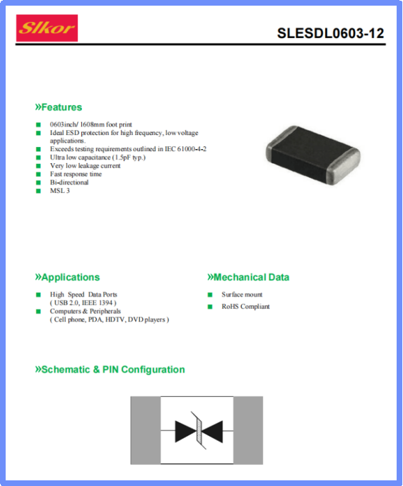
The SLESDL0603-12 transient suppression diode from Slkor provides nano-level protection matching GaN devices with the following key features:
1. 12V VRWM: Fully aligned with the standard driving voltage (8-15V) of GaN power devices, ensuring high impedance states during PWM dimming or high-frequency switching (>1MHz), with a leakage current of only 500nA.
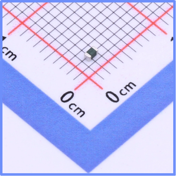
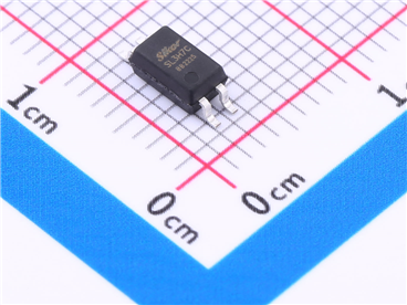
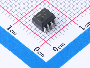
Slkor Transient Protection Diode SLESDL0603-12 product photo
2. 65V Clamping Voltage: Limits overvoltage to below the safe operating area (SOA) threshold of GaN devices, with a response time in the picosecond range—three orders of magnitude faster than traditional TVS diodes.
Slkor Transient Protection Diode SLESDL0603-12 specification
3. 0603 Package: The 0.6×0.3mm miniature size supports 3D integration and can be embedded within GaN chip-level packages (Chiplets), forming a distributed protection network.
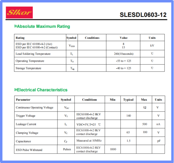
Parameters of Slkor Transient Protection Diode SLESDL0603-12
With a capacitance of less than 0.1pF, the device resolves the signal attenuation issue seen with traditional protection components in high-frequency scenarios, preserving the RF performance of GaN devices.
In Jiufengshan Lab’s GaN devices, the SLESDL0603-12 demonstrates three core values:
1. Fast Charging: In 100W USB PD chargers, it protects GaN switches from VBUS hot-plug surge impacts, increasing power density by 60% while maintaining a fault rate of less than 0.1%.
2. RF Front-End: In 5G millimeter-wave AAU modules, it absorbs nanosecond-level voltage spikes caused by antenna tuning, extending the MTTF of GaN power amplifiers (PAs) from 500 hours in lab tests to 5000 hours in commercial use.
3. Automotive Electronics: In automotive LiDAR driver circuits, it withstands transient load dump spikes defined by ISO7637-2, ensuring GaN devices remain stable in environments up to 150°C.
Real-world test data from a certain new energy vehicle manufacturer show that with the SLESDL0603-12, the ESD immunity of the GaN on-board charger improved from 2kV to 8kV, meeting the IEC61000-4-2 Level 4 standard.
As GaN technology advances towards the 50nm node, Slkor is developing intelligent protection devices with integrated temperature sensing. This new TVS diode will monitor chip junction temperatures in real-time and automatically reduce the clamping voltage once the threshold of 175°C is exceeded, forming a "self-healing" protection mechanism. In Jiufengshan Lab’s tests, this solution extended the lifespan of GaN devices under extreme thermal stress by 8 times, enabling applications in ultra-high-reliability fields such as avionics.
The 100nm GaN process breakthrough from Jiufengshan Lab is like opening a door to the world of high-frequency, high-efficiency electronics, and Slkor’s SLESDL0603-12 serves as the invisible guardian of that door. As GaN devices deliver quantum-level performance at the nanoscale, every transient voltage surge could become an "Achilles' Heel." The relationship between protection and being protected not only defines the reliability boundaries of third-generation semiconductor technology but also signals a new paradigm in future electronic engineering: material innovation and circuit protection must evolve in tandem. As power electronics move toward atomic-level precision, transient suppression diodes are writing the legendary story of the "Invisible Guardian."

Site Map | 萨科微 | 金航标 | Slkor | Kinghelm
RU | FR | DE | IT | ES | PT | JA | KO | AR | TR | TH | MS | VI | MG | FA | ZH-TW | HR | BG | SD| GD | SN | SM | PS | LB | KY | KU | HAW | CO | AM | UZ | TG | SU | ST | ML | KK | NY | ZU | YO | TE | TA | SO| PA| NE | MN | MI | LA | LO | KM | KN
| JW | IG | HMN | HA | EO | CEB | BS | BN | UR | HT | KA | EU | AZ | HY | YI |MK | IS | BE | CY | GA | SW | SV | AF | FA | TR | TH | MT | HU | GL | ET | NL | DA | CS | FI | EL | HI | NO | PL | RO | CA | TL | IW | LV | ID | LT | SR | SQ | SL | UK
Copyright ©2015-2025 Shenzhen Slkor Micro Semicon Co., Ltd
