Service hotline
+86 0755-83044319
release time:2023-12-19Author source:SlkorBrowse:16883
V. Parasitic turn-on effect of silicon carbide MOSFET and improvement measures
In the previous article, we also briefly analyzed the general requirements for gate-level drive waveforms of silicon carbide MOSFETs with a half-bridge structure. We will consider using negative voltage for reliable turn-off to avoid the impact of a smaller gate-level conduction threshold. And some unexpected gate-level coupling peak voltages cause false turn-on. However, the negative voltage withstand specifications of silicon carbide MOSFETs are not as large as those of silicon MOSFETs, so the specifications need to be strictly followed and a certain margin considered. Regarding the implementation of specific positive/negative voltage drive, there are many methods to achieve it, such as multi-channel isolated DC/DC power supply, or isolated driver IC with isolated DC/DC, etc.
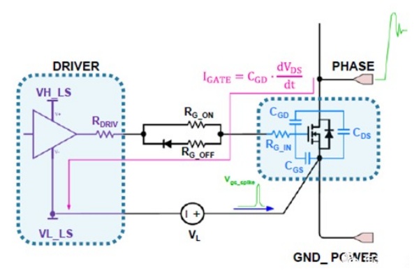
In fact, in the typical bridge circuit topology used in high-power circuits, the half-bridge structure is the basic topological unit, as shown in Figure 8. When the upper tube is turned on, that is, when the lower tube is turned off, the switching node generates a relatively large amount of energy. Large dV/dT, so this voltage will be coupled to a voltage pulse at the gate level through the silicon carbide parasitic capacitance CGD. Once this voltage pulse exceeds the gate turn-on threshold VGS-th value of the MOSFET, a false turn-on will occur, and we know that VGS -th is a negative temperature coefficient change. The higher the temperature, the lower the threshold, so this will be worsened at high temperatures. Once the lower tube is turned on by mistake, a short-circuit of the upper and lower tubes will inevitably occur, resulting in increased losses.
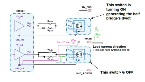
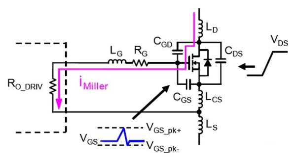
There are two situations for the gate-level peak voltage. When the upper tube is turned on and the lower tube is turned off, the lower tube will have a rapid dV/dT from low to high. Therefore, as shown in Figure 9, the node voltage passes through the CGD capacitor. Miller charging current is generated, which in turn flows through the driver's output resistor to produce a positive transient voltage at the gate level, as shown in Figure 9.
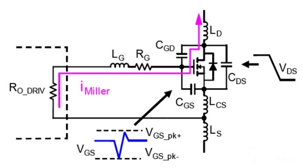
Another situation of gate-level spike is when the upper tube is turned off and the lower tube is turned on, the switching node generates dV/dT from high to low, so a reverse Miller charging current is generated, which then flows through the driver output. The resistor generates negative voltage spikes at the gate level. In this case, you need to pay attention to whether the negative voltage spike exceeds the negative voltage withstand voltage specification.
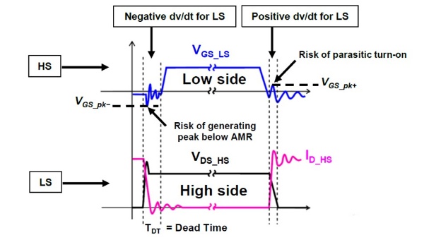
From Figure 11, we know that the gate-level oscillation before the low-side drive signal is turned on is mainly a negative voltage. This part of the voltage mainly considers the restrictions on the gate-level negative voltage specifications, while the gate-level oscillation after the low-side drive signal is turned off is mainly a positive voltage. this part of the voltage will mainly cause the half-bridge short circuit problem, so it needs to be considered.
We have clearly explained the reason why the parasitic effect is turned on, so what are the ways to suppress this effect? Generally speaking, the parasitic turn-on effect is caused by the large dV/dT of the drain, so limiting the change rate of dV/dT is a way to suppress the parasitic turn-on effect, but this conflicts with the goal of reducing switching losses.
In addition, regarding external factors, select a driver with a low pull-up resistance and set a low turn-off resistance RGoff, which allows the Miller current to pass through a lower impedance path and reduce the amplitude of the induced voltage. Of course, as mentioned in the previous article, if a negative voltage gate-level turn-off voltage is used, it can also effectively prevent the lower tube from accidentally turning on.
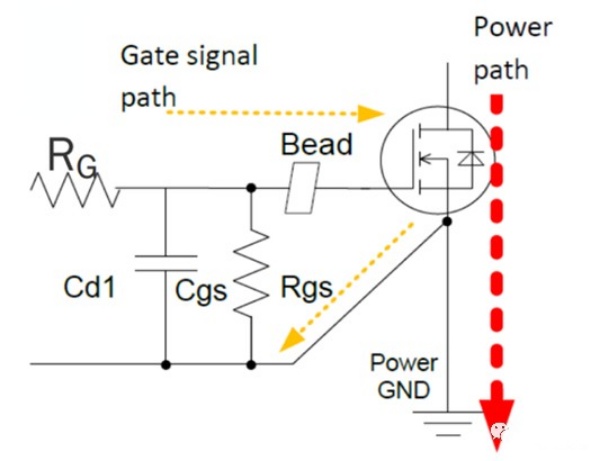
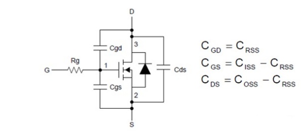
Make a fuss about the device itself, such as choosing a silicon carbide MOSFET whose CGS capacitance is much larger than the CGD capacitance. In this way, the current charging the gate-level capacitance through the Miller capacitance becomes weaker, as shown in Figure 13. Of course, you can also artificially A small capacitor is connected in parallel at the gate level to reduce the charging effect of the Miller capacitor on the gate-level capacitance, as shown in Figure 14, but it will also bring more switching and driving losses. Public data shows that under high-pressure applications, the ratio of CGS to CGD will be larger than under low-pressure applications, so it is more conducive to high-pressure applications.
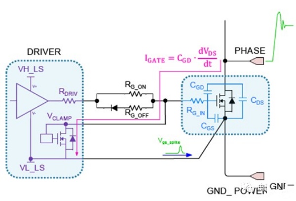
Another effective method is to use a Miller clamp circuit. When the gate voltage turn-off spike is detected, the Miller clamp circuit is turned on to clamp the gate voltage to GND, so that the Miller current will not pass through the driver output. The resistor raises the gate voltage, so that the silicon carbide MOSFET can be turned off using 0V voltage without using negative voltage to turn off. As shown in Figure 15, it is a VCLAMP circuit. Generally, this part of the circuit can be integrated into the driver chip.
VI. Considerations for short circuit protection of silicon carbide MOSFETs
An important parameter of silicon carbide MOSFET is short circuit withstand time (SCWT). Since this parameter involves device safety, it needs to be paid attention to. Due to the high current density of silicon carbide MOSFET, its chip occupies a small area, so its short-circuit withstand time is shorter than that of silicon MOSFET, so timely protection is required.
For a 1200V withstand voltage TO247 packaged silicon carbide MOSFET, under 700V conditions and 18V VGS driving voltage, its short-circuit withstand time is about 8-10uS. Turning off the silicon carbide MOSFET in such a short period of time will cause a very large dI/dT at the drain, resulting in a large drain voltage spike. In order to reduce the voltage spike, it is generally recommended to turn off the silicon carbide MOSFET slowly when a short circuit occurs and a large current occurs. cut off the VGS voltage.
In terms of specific implementation, sampling is generally performed through a current sampling resistor, and a desaturation action is performed on the short-circuited silicon carbide MOSFET. However, the disadvantage of this is that it causes additional losses, and the sampling circuit will increase the PCB space, so it is only used for Low power applications are shown in Figure 16. In high-power applications, the Vds voltage is generally used as the sampling voltage to trigger the overcurrent protection and desaturate the device. However, the accuracy of this method is not that high because the Vds obtained by Rdson sampling current has a certain range of variation, as shown in the figure 17 shown.
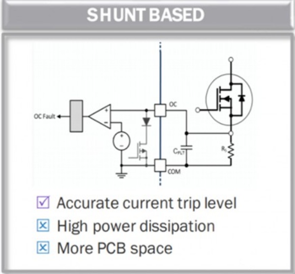
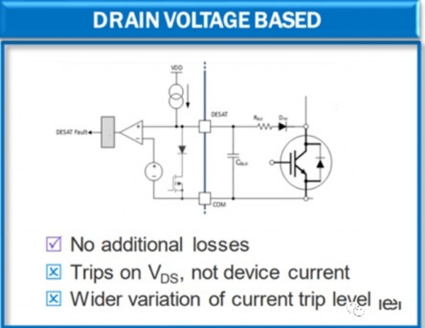
Using Vds sampling to design an overcurrent protection circuit is a very particular matter, because it is necessary to take into account both the timeliness of the trigger protection and the avoidance of false triggers. For the former, the worst case scenario of Rdson, as well as temperature and other factors need to be considered.
The typical detection desaturation time is generally around 250n-500nS when the signal is detected after the circuit is turned on, and it takes about 400n-1500nS to turn off the protection. In fact, it needs to be detected when saturation has not occurred (or the current has not yet been reached). before the peak value), you need to be able to detect the current signal, and cannot wait until saturation occurs before detecting the current signal.
VII. Considerations on silicon carbide MOSFET power device packaging
In high-voltage and high-power applications, plug-in packages such as TO220 or TO247 will be used. Therefore, during use, the length of the pins should be reduced as much as possible to reduce the parasitic inductance caused by the device packaging.
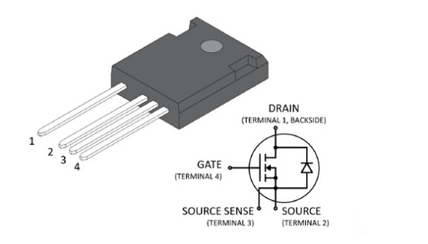
As discussed earlier in the parallel design of silicon carbide MOSFETs, wiring the MOSFET sources separately to the drive circuit will significantly reduce switching losses. The reason is that the source parasitic inductance will slow down the turn-on process or turn-off process and increase switching losses. Therefore, generally speaking, the TO247-4 package will have 30% less switching loss than the TO247 package.
To analyze this process specifically, we take the upper tube of the half-bridge as an example, as shown in Figure 18 (move Figure 8 here). When the switch is turned on, the current flows from top to bottom and gradually increases, then the source The induced voltage is positive on the upper side and negative on the lower side. This voltage will reduce the gate drive voltage, thus slowing down the turn-on process. Similarly, when the upper transistor is turned off, the current flows from top to bottom and gradually decreases, so the source induced voltage is positive below and negative above. This will increase the source drive voltage and therefore slow down the turn-off process. Both states will increase switching losses, so if switching losses dominate or are large, consider using TO247-4 packaging.

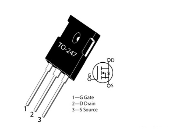
From the package diagram, as shown in Figure 19, the TO247-4 package has a separate source connection pin3, which is adjacent to the Gate pin to facilitate the application of drive signals, and the distance between the drain pin1 and the source pin2 is very small. Large, it needs to withstand the Vds high voltage. The pin arrangement of TO247 is relatively simple, with G gate, D drain and S source arranged in order.
In different packages of silicon carbide MOSFET modules, reasonable design to obtain smaller parasitic inductance is very helpful in limiting voltage overshoot, and at the same time, it will also increase the product's operating switching frequency as much as possible.
Through the discussion of the above seven parts, from the basic requirements of isolation drive, to the calculation of drive loss, from the parasitic turn-on effect of a single tube, to the implementation of multi-tube parallel connection, and the corresponding layout principles, several precautions are finally reminded from the packaging. I hope everyone can have a more thorough understanding of the silicon carbide MOSFET drive circuit so that it can be implemented in actual solutions to give full play to the performance of the silicon carbide MOSFET.



Site Map | 萨科微 | 金航标 | Slkor | Kinghelm
RU | FR | DE | IT | ES | PT | JA | KO | AR | TR | TH | MS | VI | MG | FA | ZH-TW | HR | BG | SD| GD | SN | SM | PS | LB | KY | KU | HAW | CO | AM | UZ | TG | SU | ST | ML | KK | NY | ZU | YO | TE | TA | SO| PA| NE | MN | MI | LA | LO | KM | KN
| JW | IG | HMN | HA | EO | CEB | BS | BN | UR | HT | KA | EU | AZ | HY | YI |MK | IS | BE | CY | GA | SW | SV | AF | FA | TR | TH | MT | HU | GL | ET | NL | DA | CS | FI | EL | HI | NO | PL | RO | CA | TL | IW | LV | ID | LT | SR | SQ | SL | UK
Copyright ©2015-2025 Shenzhen Slkor Micro Semicon Co., Ltd