Service hotline
+86 0755-83044319
release time:2023-09-09Author source:SlkorBrowse:8228
Van den Hove stated that the industry will require a wide range of technological options and combinations to achieve specific technical solutions that meet the requirements of specific workloads and systems. "Interposer chips and tiny silicon bridge interposers will allow very fast connections between multiple core processor chiplets and 3D DRAM memories," he said.
Today, DRAM memories are typically built in 3D layer stacks, while core processor chiplets are manufactured using a single chip (a single 2D chip system). "The next approach to achieve heterogeneous integration is building advanced 2D processor chips as 3D layer stacks, dividing functionality into multiple layers. This can be accomplished using advanced wafer stacking technologies, such as through-silicon via technology and copper-to-copper hybrid bonding, enabling very high-density interconnects between the logic layer and the memory cache layer," Van den Hove said. Figure 5 illustrates this in practice.
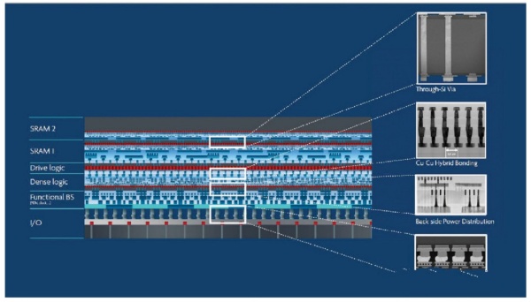
Figure 5
"We believe that this will be one of the ways to further extend Moore's Law beyond what we thought possible. We call this roadmap CMOS2.0, achieving the next phase of Moore's Law through further 2D scaling enabled by 3D stacking. 3D alone will only bring us linear increases in complexity," said Van den Hove.
Another issue is that the power consumption of advanced chips continues to increase to the point where extracting heat from the chip poses some limitations. "Clearly, to realize such complex 2D and 3D stacked core processor architectures, we need to address the thermal challenge and learn how to cool chips more efficiently. To do so, we are developing innovative cooling systems that can be manufactured using 3D printing technology," Van den Hove said. This direct liquid jet impingement cooling achieves higher heat dissipation efficiency, five times higher than the currently most advanced technologies.
Song from Samsung highlighted trends particularly relevant to logic, DRAM, and NAND device structures. In terms of logic products, he mentioned that Samsung is developing backside interconnection to address the challenge of unit height scaling. "Furthermore, innovations in structures and materials, such as channel materials with optimal layer thickness, can provide excellent gate controllability compared to silicon channels," he said (see Figure 6).
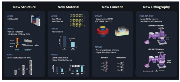
In DRAM, Samsung is researching vertical channel stacking 3D structures to address the challenge of lateral scaling, which, according to Song, differs greatly from existing 2D structures. "We are also trying to introduce all low leakage channel materials rather than the leakage control silicon channels that have been used so far," he said. "To overcome unit capacitor issues, we are studying new concepts for capacitor-less DRAM."
In NAND, technologies such as multi-stack will continue to evolve. "New materials are needed to overcome mechanical stress or sensing margins. To further shrink the unit device size, new concepts for device development that can lower operating voltage are needed," said Song. "To improve the resolution and uniformity of EUV, high numerical aperture EUV technology with larger mirrors is also needed."
The need for innovation and collaboration
"In order to continue advancing in the digital transformation era, the technologies for storing and processing such large amounts of data require development in the new era, and the semiconductor industry needs continuous innovation to make this possible," said Song.
Papermaster from AMD pointed out that just a decade ago, deep neural networks began showing prospects for accelerating computing. "There is no doubt that we are still in the early stages," he said. "But I am very hopeful because I know that if we take the right policies and constraints, we will see in the coming years a transformation that will make our city even more incredible and productive. We will leverage AI-driven computing to accelerate innovation."
Van den Hove emphasized the need for a "moonshot" mindset. "This requires rapid development and collaboration across the entire value chain and continents, bringing together the best talents. Just like the moon landing mission of the 1960s, we face seemingly insurmountable challenges. We must once again unite and build a rocket fueled by innovation. But now, our goal is not just the moon, our goal is a better planet, to have a better life on Earth."



Site Map | 萨科微 | 金航标 | Slkor | Kinghelm
RU | FR | DE | IT | ES | PT | JA | KO | AR | TR | TH | MS | VI | MG | FA | ZH-TW | HR | BG | SD| GD | SN | SM | PS | LB | KY | KU | HAW | CO | AM | UZ | TG | SU | ST | ML | KK | NY | ZU | YO | TE | TA | SO| PA| NE | MN | MI | LA | LO | KM | KN
| JW | IG | HMN | HA | EO | CEB | BS | BN | UR | HT | KA | EU | AZ | HY | YI |MK | IS | BE | CY | GA | SW | SV | AF | FA | TR | TH | MT | HU | GL | ET | NL | DA | CS | FI | EL | HI | NO | PL | RO | CA | TL | IW | LV | ID | LT | SR | SQ | SL | UK
Copyright ©2015-2025 Shenzhen Slkor Micro Semicon Co., Ltd