Service hotline
+86 0755-83044319
release time:2023-10-11Author source:SlkorBrowse:8865
Could our lives last a day without semiconductors? Many aspects of our daily lives, including smartphones, laptops, cars, televisions, and credit cards, are inseparable from semiconductors. These semiconductors have a profound impact on our lives. So, how are they made?

If you have some basic knowledge of semiconductors, you may have heard of the eight fundamental semiconductor processes. Numerous tasks required for semiconductor manufacturing are divided into eight basic processes, as indicated by the title in the first image of our article: "Eight Fundamental Semiconductor Processes."
Today, we will take a look at the first step, "Wafer Manufacturing." We will discuss what wafers, the core material of integrated circuits, are made of, and how they are manufactured.
Materials Required for Wafer Manufacturing
Before we begin, let's ask a brief question! What is the relationship between semiconductor integrated circuits and wafers? An integrated circuit is a type of semiconductor chip that contains numerous electrical components for various functions. Integrated circuits are manufactured by creating many identical circuits on a substrate called a wafer. Therefore, wafers are the foundation of semiconductors. This is similar to making pizza - we prepare a dough first so that we can add toppings later.
Wafers are circular disks cut from silicon wafers or other elements such as gallium arsenide. Most wafers are made from silicon extracted from sand.
The Silicon Valley in the United States started with the semiconductor industry, eventually becoming the center of the global software industry. It is reported that its name is a combination of the semiconductor raw material "silicon" and the "valley" of Santa Clara. The name "Silicon Valley" may help you remember that silicon is an essential raw material for semiconductor wafers. Silicon is abundant in supply, is the most abundant element in nature, and has non-toxic and environmentally friendly properties. Let's take a look at the process of wafer manufacturing together!
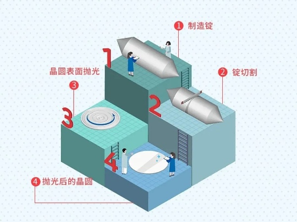
Step 1: Silicon Ingot Manufacturing
The silicon extracted from sand needs to go through a purification process before it can be used for semiconductor manufacturing. It is heated until it melts into a high-purity liquid and then solidified through crystallization. The resulting silicon rod is called a silicon ingot. Only ingots with ultra-high purity can be used in semiconductor processes, which require extremely high precision down to a few nanometers.
Step 2: Cutting Ingots to Produce Thin Wafers
The shape of the silicon ingot resembles a spinning top, and it is cut into uniformly thick circular discs, known as wafers, using sharp diamond saw blades. The diameter of the ingot determines the size of the wafer, such as 150mm (6 inches), 200mm (8 inches), and 300mm (12 inches) wafers. Thinner wafers result in lower manufacturing costs, and larger diameters allow for a greater number of semiconductor chips to be produced per wafer. Therefore, wafers are becoming increasingly thinner and larger.
Step 3: Grinding and Polishing the Wafer Surface
The freshly cut wafers need to undergo processing to achieve a smooth, mirror-like finish. The surface of the freshly cut wafer is rough and contains defects, which can have a negative impact on circuit accuracy. Polishing fluids and polishing machines are used to polish the wafer surface.
Before further processing, the polished wafer is referred to as a bare wafer, indicating that no chips have been manufactured on it yet. After the fabrication of integrated circuits on the bare wafers using various physical and chemical processes, the wafer eventually looks like the image below. Let's take a look at the names of the different parts of a wafer together!
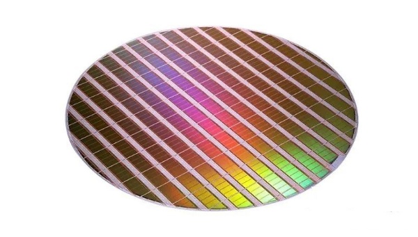

1. Wafer: A circular plate (disc) that serves as the core material for semiconductor ICs.
2. Die: There are many small squares on the wafer, and each small square is called a die, which is the IC chip of the integrated electronic circuit.
3. Scribe line: The dies appear to be stuck together, but there are actually gaps between them. These gaps are called scribe lines. The purpose of scribe lines is to cut out each chip from the wafer after processing and assemble them into chips. The spacing of the scribe lines allows the diamond saw to safely cut the wafer.
4. Flat zone: This area is introduced to help identify the wafer structure and serves as a reference line during the wafer processing. Since the crystal structure of the wafer is very fine and cannot be judged by the naked eye, this flat zone is used as a reference for determining the vertical and horizontal directions of the wafer.
5. Notch: Recently, wafers with notches have appeared, replacing the previous flat zones. Wafers with notches are more efficient than those with flat zones because they can produce more chips.
The semiconductor industry is mainly divided into the wafer manufacturing industry, which manufactures wafers, and the manufacturing (FAB) industry, which designs and manufactures circuits on the wafers. There is also the packaging industry, where processed wafers are cut into chips and packaged to prevent moisture and physical damage.
Today, we introduced what a wafer is, the names of each part of a wafer, and how wafers are manufactured. We hope you find this series of eight basic semiconductor processes interesting and helpful.



Site Map | 萨科微 | 金航标 | Slkor | Kinghelm
RU | FR | DE | IT | ES | PT | JA | KO | AR | TR | TH | MS | VI | MG | FA | ZH-TW | HR | BG | SD| GD | SN | SM | PS | LB | KY | KU | HAW | CO | AM | UZ | TG | SU | ST | ML | KK | NY | ZU | YO | TE | TA | SO| PA| NE | MN | MI | LA | LO | KM | KN
| JW | IG | HMN | HA | EO | CEB | BS | BN | UR | HT | KA | EU | AZ | HY | YI |MK | IS | BE | CY | GA | SW | SV | AF | FA | TR | TH | MT | HU | GL | ET | NL | DA | CS | FI | EL | HI | NO | PL | RO | CA | TL | IW | LV | ID | LT | SR | SQ | SL | UK
Copyright ©2015-2025 Shenzhen Slkor Micro Semicon Co., Ltd