Service hotline
+86 0755-83044319
release time:2023-09-05Author source:SlkorBrowse:14049
Currently, most 100mm and 150mm wafers in the semiconductor industry are made of single-crystal silicon carbide with a hexagonal lattice structure (represented by 4H and 6H for 4-inch and 6-inch wafers, respectively). However, major SiC device manufacturers are successfully transitioning from 150mm to 200mm wafers, and other manufacturers are also capitalizing on this supply.
For example, according to analysts from Yole Group, Infineon sources wafers from multiple suppliers, including STMicroelectronics, which acquired a majority stake in Swedish company Norstel. Silicon power device supplier Rohm is ramping up its capacity and partnerships. In July, Rohm signed a 10-year agreement and paid a $2 billion deposit to Wolfspeed for the supply of 150mm bare and epitaxial SiC wafers. Rohm also reached an agreement with Mitsubishi, which will invest 260 billion Japanese yen in technology and expansion, including the construction of a SiC plant in Japan.
"Rohm is a newcomer in the traditional power semiconductor field, but now [our products] are gaining attention for their high efficiency," said Hidetoshi Shibata, the company's president, in a recent press release. "SiC can achieve that as well."
Meanwhile, SOITEC and STMicroelectronics are exploring a method called multi-crystalline SiC on single crystal substrates, which involves dividing single crystal silicon wafers into multiple slices and reusing donor wafer substrates to reduce waste. The advantage of multi-crystalline silicon substrates is the ability to conduct heat through the substrate to metal connectors, enabling faster switching and excellent heat dissipation.
In some aspects, silicon carbide is following the development trajectory of silicon. However, due to the defect levels in SiC, data sharing is necessary.
"We exchange raw material data and equipment data with silicon wafer suppliers," said Bornefeld from Bosch. "We also use advanced AI-based systems to identify good correlations and share this information so that both companies can move forward."
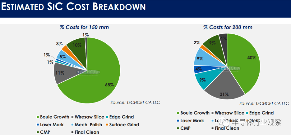
Nevertheless, data sharing is not yet widespread. Unlike silicon, the transition from 150mm to 200mm ingot size does not bring significantly higher returns in terms of wafer/ingot forms. Additionally, 200mm requires larger seed crystals, which take longer to grow at 2,500°C. Currently, the increase in productivity (wafers/ingots) may be in the range of 20%. Analysts from TECHCET estimate that the cost contribution of ingot growth will decrease compared to slicing, grinding, polishing, and CMP processes.
The demand for automotive chips exceeds that of electric vehicles
STMicroelectronics' Marketing Director for Automotive Intelligent Power and Discrete Products, Lee Bell, stated, "We are seeing the demand for automotive semiconductor applications growing faster than the increase in electric vehicle production." "This is due to various factors. Advanced driver safety features, autonomous vehicle control, advanced connectivity, and convenience functions are all driving the demand for semiconductors, but in a different way than the electrification of power systems," he said. "By 2022, about two-thirds of electric vehicles will be hybrid, with about one-third being battery-driven. By 2030, this trend will reverse. This is due to increased market acceptance, improved availability of charging infrastructure, but perhaps most importantly, this is where automakers are placing their research and manufacturing budgets." This change is a key driving force for the use of SiC MOSFETs.
Bell pointed out that traction inverters often use larger chips. He added that power semiconductors are huge consumers in the vehicle's charging system and the DC-DC converter that reduces voltage from the battery to the Internet of Things system. Both of these are absent in hybrid vehicle architectures.
He also emphasized that efficiency (packaging devices and modules) is of primary concern because the less power loss in the system, the longer the range of the car and truck. "We conducted a study comparing a 210kW inverter system (approximately equivalent to 280 horsepower) with SiC MOSFETs and silicon IGBTs," he said. "The silicon carbide method consistently delivers 98% operational efficiency, while the IGBT method is less efficient, especially in the low operating load range, where the vehicle spends about 95% of its life."
Total power is the sum of conduction losses and switching losses. "Silicon carbide reduces switching losses by a factor of four," he said. ST is currently producing its fourth-generation SiC products with an improved RDSon performance of 30%.
Bosch's Bornefeld presented demand and capacity forecasts for 2030, indicating substantial global wafer and wafer fab capacities in Japan, South Korea, China, Malaysia, Germany, Austria, and the United States. In fact, the industry needs to be cautious not to overbuild (see Figure 5). "The question is, 'What's happening in China?' China is already leading in silicon carbide raw materials, and they are providing wafers of very high quality at reasonable prices," Bornefeld said. "They are also rapidly catching up in terms of equipment. So, we do need to watch and track overall capacity."
Finally, Veliadis from PowerAmerica talked about the workplace training required for skilled implementation of wide-bandgap semiconductors such as SiC and GaN in wafer fabs. "There is a high demand for engineers with expertise in SiC and GaN MOSFET manufacturing, and there are significant differences between SiC wafer fabs and silicon wafer fabs," he said.
Conclusion
The transition to clean energy and electric vehicles will require alternative semiconductor materials such as SiC and GaN, and power devices are sure to undergo significant optimization in the coming decades. The frenzy of technological improvements and capacity expansions may not continue, but power devices will still be a key part of many companies' roadmaps.
"We know that the semiconductor industry is moving towards a $1 trillion market, but everyone wants to know what will happen after 2030," said David Britz, Strategic Marketing Director at Applied Materials ICAPS. "I'm here to prove that the fifth era of semiconductors is indeed driven by the transformation of energy production and transportation."
Managing the growth of SiC wafers, devices, and modules may be the most challenging aspect of the SiC market to date, along with supply chain issues, filling technological gaps, and geopolitical changes. Nevertheless, the semiconductor technology industry seems to have reached a consensus on many things, especially regarding the demand for next-generation power efficiency and performance.



Site Map | 萨科微 | 金航标 | Slkor | Kinghelm
RU | FR | DE | IT | ES | PT | JA | KO | AR | TR | TH | MS | VI | MG | FA | ZH-TW | HR | BG | SD| GD | SN | SM | PS | LB | KY | KU | HAW | CO | AM | UZ | TG | SU | ST | ML | KK | NY | ZU | YO | TE | TA | SO| PA| NE | MN | MI | LA | LO | KM | KN
| JW | IG | HMN | HA | EO | CEB | BS | BN | UR | HT | KA | EU | AZ | HY | YI |MK | IS | BE | CY | GA | SW | SV | AF | FA | TR | TH | MT | HU | GL | ET | NL | DA | CS | FI | EL | HI | NO | PL | RO | CA | TL | IW | LV | ID | LT | SR | SQ | SL | UK
Copyright ©2015-2025 Shenzhen Slkor Micro Semicon Co., Ltd