Service hotline
+86 0755-83044319
 en
en release time:2023-10-13Author source:SlkorBrowse:11858
II. DUV and LPP-EUV Light Sources
The chip manufacturing process described above is applicable to both traditional chips (28nm and above) and advanced process chips (14nm and below). Currently used photolithography machines use mainly DUV light sources, with a light source generator producing ArF (argon fluoride) excimer lasers at a wavelength of 193nm. Immersion lithography machines refract light in water to a wavelength of 134nm.
Earlier, mercury lamp light sources (not lasers) were used. G-line photolithography machines use a wavelength of 436nm, while i-line photolithography machines use a wavelength of 365nm. There are also KrF (krypton fluoride) excimer laser generators with a 248nm light source.
According to the Rayleigh criterion formula and practical results, the resolution of a 193nm photolithography machine is one-third of the wavelength, which can be used to make 65nm chips. An immersion lithography machine with a 134nm wavelength, according to the rule, can be used to make 45nm chips. However, the effect of the lens in water is increased, and the final resolution capability is increased to 28nm through the OPC compensation algorithm (making specific complex shapes rather than the original square on the mask pattern, resulting in a more square-like final image). This is the origin of the classic 28nm chip, and there is a saying in the industry about "28nm photolithography machines," which is actually a 193nm light source.
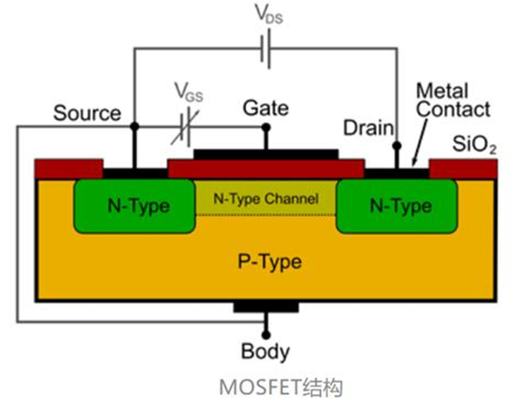
Traditional chips with a process node of 28nm and above typically utilize MOSFET (Metal-Oxide-Semiconductor Field-Effect Transistor) transistors. These transistors can be understood as planar transistors, featuring a control gate that allows voltage to be applied from top to bottom in a single direction, controlling the transistor's conductivity state between 0 and 1. The term "28nm" refers to the width between the source and drain electrodes, with the entire transistor being over 100nm wide.
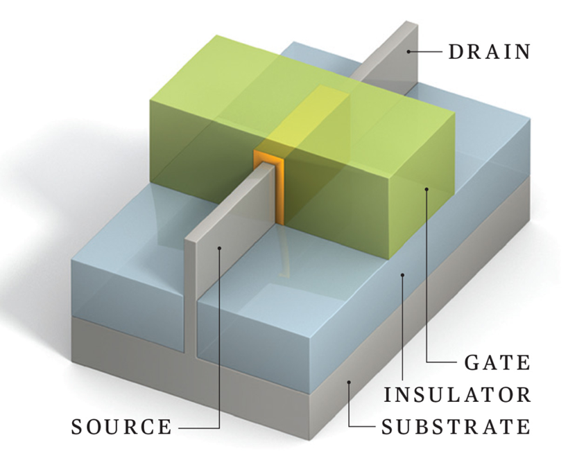
The FINFET transistor is upgraded to a "3D" structure, as shown in the figure. The green Gate applies voltage from three directions: top, left, and right, to influence the conduction state of the transistor. The 3D influence from three directions is more sensitive than the planar influence from one direction in MOSFET, resulting in lower power consumption and higher frequency in FINFET transistors. However, this transistor requires the fin to be thin and extend upwards like a fish fin, making the fabrication process more complex. It is important to note that FINFET transistors are still arranged in a flat manner on the wafer, with multiple transistors, but the fins have a 3D structure that is sensitive to the control voltage.
Using DUV immersion lithography machines and FINFET transistor technology, chips with a 7nm-14nm process can be fabricated. The main method is multiple exposures, up to four exposures. To simplify, first create lines with intervals of 28-28-28-28nm on the wafer, then shift by 14nm and create another set of lines with intervals of 28-28-28-28nm, which can combine into lines with intervals of 14-14-14-14nm using double exposure. With four exposures, lines with intervals of 7-7-7-7nm can be achieved. Of course, this is just an analogy, the actual process is much more complex, but the basic principle is to divide the tasks originally done by a single mask into multiple masks. At 7nm, the process becomes very complicated, requiring a large number of masks, but outstanding companies in the industry have actually achieved mass production of 7nm chips using DUV lithography machines.
It is worth noting that for traditional chips with a process of 28nm and above, the "process" is as real as it gets, meaning the actual gate length is 28nm. However, for advanced chips with a process of 7nm-14nm, including 5nm, 4nm, and 3nm chips, the gate width is not the nominal value. Each chip manufacturer claims their own "equivalent area" (PPA, Power Performance Area) based on improvements in power consumption and other performance indicators, which may result in a measured gate width of 10nm despite being labeled as 7nm. Intel's 10nm process is indeed true to its name; when they say it's 10nm, its metrics are equivalent to 7nm from other companies.
As can be seen, using DUV lithography machines to create 7nm chips has exhausted all tricks to achieve the desired effect using a 193nm light source. Immersion lithography, lens improvements, OPC compensation, multiple exposures, 3D transistor structure, and equivalent area have collectively achieved the 7nm effect using a 193nm light source. The process of fabricating advanced chips using DUV lithography machines is very complicated, with low yields and high costs.
To be continued...



Site Map | 萨科微 | 金航标 | Slkor | Kinghelm
RU | FR | DE | IT | ES | PT | JA | KO | AR | TR | TH | MS | VI | MG | FA | ZH-TW | HR | BG | SD| GD | SN | SM | PS | LB | KY | KU | HAW | CO | AM | UZ | TG | SU | ST | ML | KK | NY | ZU | YO | TE | TA | SO| PA| NE | MN | MI | LA | LO | KM | KN
| JW | IG | HMN | HA | EO | CEB | BS | BN | UR | HT | KA | EU | AZ | HY | YI |MK | IS | BE | CY | GA | SW | SV | AF | FA | TR | TH | MT | HU | GL | ET | NL | DA | CS | FI | EL | HI | NO | PL | RO | CA | TL | IW | LV | ID | LT | SR | SQ | SL | UK
Copyright ©2015-2025 Shenzhen Slkor Micro Semicon Co., Ltd
