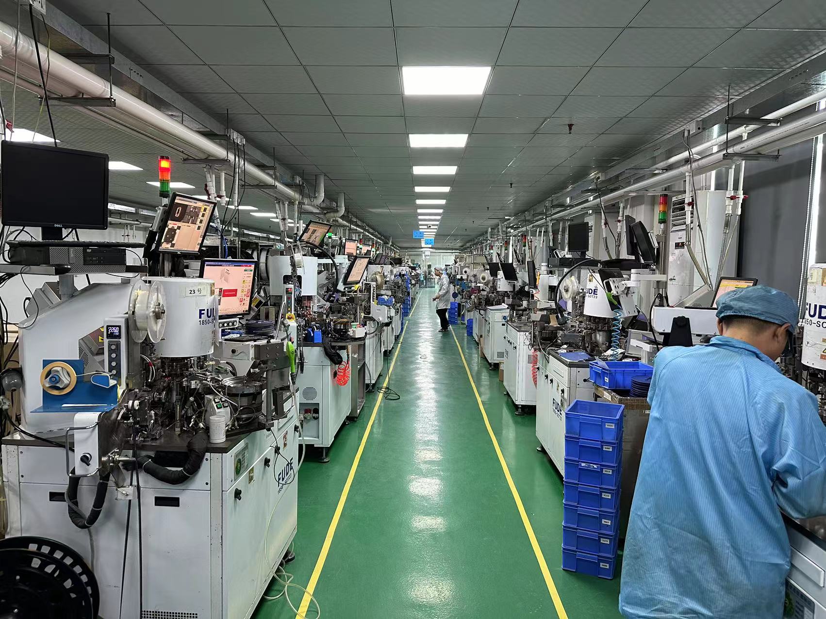
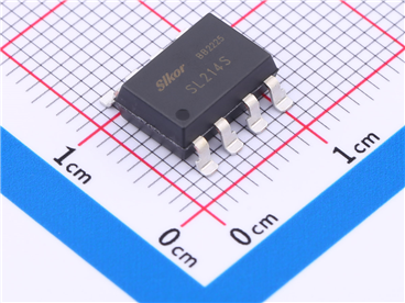
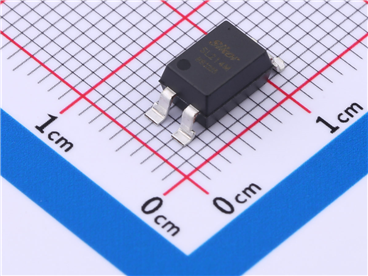
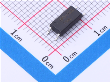
Due to the complexity of semiconductor manufacturing processes, different equipment is required for various steps. From a process classification perspective, semiconductor equipment can be mainly divided into silicon wafer production process equipment, wafer manufacturing process equipment, packaging process equipment, etc. These devices correspond to different processes in IC production, used in different stages of the IC production process.
Based on the sales revenue of various types of IC equipment, in the entire semiconductor equipment market, wafer manufacturing equipment accounts for 81%, packaging equipment accounts for 6%, testing equipment accounts for 8%, and other equipment accounts for 5%. Within wafer manufacturing equipment, lithography machines, etching machines, and thin film deposition equipment are core devices, roughly accounting for 24%, 24%, and 18% of the wafer manufacturing equipment costs, respectively.

Lithography Machine
In the semiconductor chip fabrication process, lithography is a crucial step, with lithography machines being the most precise, complex, and expensive equipment in semiconductor chip manufacturing. They serve as a key indicator of the overall manufacturing process's advancement.
Currently, the most widely used machines are immersion lithography machines and EUV lithography machines. EUV lithography machines represent the latest technological advancement. They were developed to address the shrinking process nodes where traditional lithography techniques were insufficient, necessitating costly double patterning and resulting in escalating equipment and production costs, marking a departure from Moore's Law and a rise in transistor unit costs.
Although EUV lithography machines have started shipping, their high cost and long lead times make them challenging for most companies to procure. Therefore, the lithography machine market is currently dominated by 193nm ArF lithography machines.
Etching Machine
Etching is a critical process in IC manufacturing that involves pattern transfer following lithography. It uses the lithography mask pattern as a template to selectively remove material from the substrate, creating IC patterns.
Etching techniques are classified into wet etching and dry etching processes, with dry etching, particularly plasma etching, being the mainstream technology. Plasma etching machines are large, fully automated processing units operating in a vacuum environment. These machines utilize excited ions and chemically reactive neutral atoms in a low-temperature plasma to etch materials.
Dry etching is further divided into capacitive plasma etching and inductive plasma etching, with each catering to specific material characteristics and process requirements.
Thin Film Deposition Equipment
Thin film deposition is a process involving atomic adsorption, diffusion, and nucleation on a substrate to deposit a layer of film. Deposition methods include physical vapor deposition (PVD) and chemical vapor deposition (CVD).
PVD and CVD technologies have their advantages and disadvantages. PVD involves heating source materials to evaporate atoms or molecules onto the substrate, including techniques such as vacuum evaporation and sputtering. On the other hand, CVD utilizes thermal energy, plasma discharge, or UV radiation to induce chemical reactions for film deposition.
