Service hotline
+86 0755-83044319
release time:2023-09-11Author source:SlkorBrowse:8378
The current design direction for SiC modules is to achieve a more compact structure. This is accomplished through the use of double-sided silver sintering and copper wire bonding technologies, as well as the design of high-performance aluminum nitride (AlN) ceramic substrates for liquid-cooled copper base PinFin boards, and induction terminals for multi-signal monitoring (compatible with welding and press-fitting). Efforts are being made to achieve low losses, high breakdown voltage, low on-state resistance, high current density, and high reliability. Good design and advanced process technology ensure that the advantages of silicon carbide MOSFETs are maximized in devices.
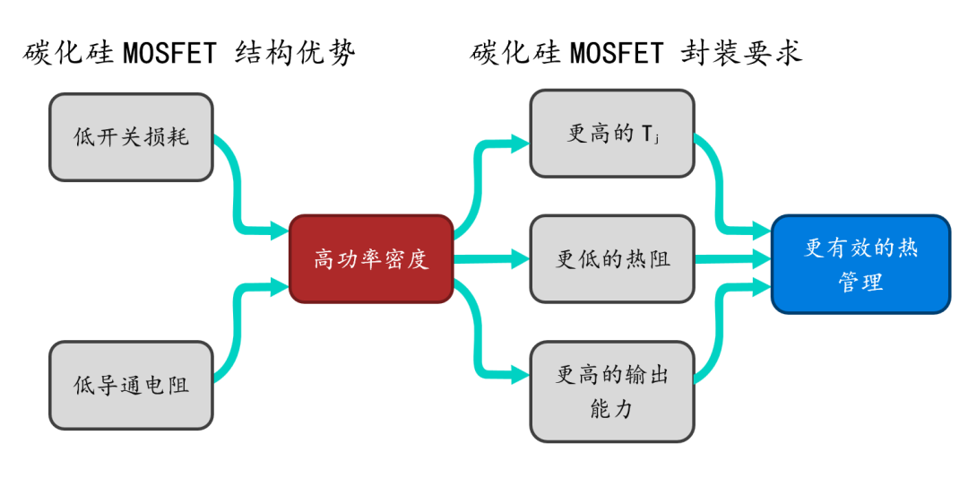
Smaller cell size, lower on-resistance, lower switching losses, and improved gate oxide protection are the main development trends of silicon carbide (SiC) MOSFET technology. These trends reflect in better performance and higher reliability in application. Moreover, the high power density, high junction temperature characteristics, and high-frequency requirements of SiC devices also raise higher demands on existing packaging technologies. Currently, power module packaging innovation in China is mainly focused on the following directions:
Advanced connection materials and processes to withstand higher temperature variations:
The main three types of ceramic-copper substrates used in power modules are as follows: AI2O3-DBC has the highest thermal resistance but the lowest manufacturing cost; AlN-DBC has the lowest thermal resistance but poor toughness; Si3N4-AMB ceramic material has intermediate thermal resistance, excellent toughness, and outstanding thermal capacity parameters, which greatly enhances the module's heat dissipation capability, current-carrying capacity, and power density. Si3N4-AMB is particularly suitable for automotive-grade SiC module applications.
Shorter interconnection paths and advanced interconnection technologies to reduce parasitic inductance for high-frequency device characteristics:
Silver sintering is currently the most advanced welding technology in the field of SiC modules. It can fully meet the demanding requirements of automotive-grade power modules for high and low-temperature operating conditions. Compared to traditional soldering techniques, silver sintering achieves zero voids, low-temperature sintering for high-temperature service, and reduces the solder layer thickness by 60-70%. It is suitable for high-temperature device interconnections. Silver sintering offers better electrical and thermal performance compared to soldering materials, with a 5-6 times increase in electrical conductivity and a 3-4 times increase in thermal conductivity. Many companies have already attempted to upgrade all traditional solder materials inside power modules, including chips, resistors, and sensors, to silver sintering processes.
Integration of packaging structure design and circuit topology for better system thermal management:
In order to make the thermal path design of module products more compact and enable more compact and efficient integrated design of inverter systems, as well as further reduce the overall system costs, improvements in heat dissipation and current-carrying capacity are achieved through changes in packaging forms. Internal structures with multiple parallel-connected chips are used, where the main parallel circuits and driving circuits have similar parameters to ensure the current sharing among parallel chips. Temperature sensors (PTCs) are installed inside the module, and the PTCs are placed near the chips at the center position of the module, enabling close thermal coupling and convenient and accurate temperature measurements of the module.



Site Map | 萨科微 | 金航标 | Slkor | Kinghelm
RU | FR | DE | IT | ES | PT | JA | KO | AR | TR | TH | MS | VI | MG | FA | ZH-TW | HR | BG | SD| GD | SN | SM | PS | LB | KY | KU | HAW | CO | AM | UZ | TG | SU | ST | ML | KK | NY | ZU | YO | TE | TA | SO| PA| NE | MN | MI | LA | LO | KM | KN
| JW | IG | HMN | HA | EO | CEB | BS | BN | UR | HT | KA | EU | AZ | HY | YI |MK | IS | BE | CY | GA | SW | SV | AF | FA | TR | TH | MT | HU | GL | ET | NL | DA | CS | FI | EL | HI | NO | PL | RO | CA | TL | IW | LV | ID | LT | SR | SQ | SL | UK
Copyright ©2015-2025 Shenzhen Slkor Micro Semicon Co., Ltd