Service hotline
+86 0755-83044319
release time:2023-09-05Author source:SlkorBrowse:13055
Key players in chip manufacturing include Wolfspeed, STMicroelectronics, ON Semiconductor, ROHM, Infineon, and Bosch. The largest cost contributor for these devices, silicon carbide (SiC) wafers, is moving from 150mm to 200mm manufacturing, but the growth, slicing, and preparation processes still rely on expensive and time-consuming manual operations.
All parties, especially IDM and wafer fabs, are striving to reduce the defect rate of SiC crystals, developing dedicated tool platforms for SiC, such as high-temperature ion implantation, epitaxial deposition furnaces operating at temperatures above 1,500°C, and improved CMP slurries, polishing pads, and cleaning chemicals for processing materials almost as hard as diamond.
As power circuits based on silicon, SiC, and GaN all compete within the 400V battery range, the technology transition has been completed. However, SiC power systems can provide much higher power levels compared to GaN (see Figure 3).
"I call it the 650V battleground because, in reality, all three technologies are competitive within this range," says PowerAmerica's Veliadis, who attended the "Connecting the Automotive Ecosystem with SiC Manufacturing" forum held at SEMICON West. While GaN has a higher electron mobility than SiC, its maturity is lower and cannot match the high power levels of SiC. However, GaN still holds significant appeal in manufacturing high-frequency devices. Additionally, some silicon-based GaN methods currently employed by companies like Intel and imec show great promise.
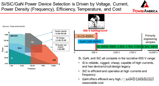
Silicon carbide (SiC) modules are considered crucial for improving the efficiency of electric vehicle powertrain systems. The significant shift from silicon-based devices to silicon carbide devices will greatly contribute to increasing power density in power systems while reducing the size, weight, and most importantly, the cost of electric vehicles. This is because although silicon-based power semiconductors are still being optimized, they have reached their operational limits in terms of conduction and switching losses. Silicon carbide, with its wider bandgap (3.26eV compared to silicon's 1.12eV), can reduce such losses and provide excellent high-temperature and high-frequency performance.
Many SiC chip manufacturers have already transformed their 150mm silicon production lines into SiC manufacturing. Veliadis stated, "The highly successful approach so far has been processing silicon carbide in mature, fully depreciated silicon factories, with a capital investment of around $30 million, yielding tremendous returns." Cost is particularly important for power modules. "By using silicon carbide, you will pay approximately three times the cost for semiconductor chips, but the overall system cost ends up being lower than that of silicon power modules, which goes against intuition. But the answer is simple. The ability to operate efficiently at high frequencies significantly reduces the volume of magnetic and passive components, offsetting the higher cost of chip manufacturing."
However, there are no old factories left that can afford a $30 million renovation in this industry. New silicon carbide wafer factories are rapidly under construction. Meanwhile, non-wafer companies are competing for capacity.
"We have two mutually competing markets—the automotive market and the renewable energy market, both seeking capacity," said Ralf Bornefeld, Senior VP of Bosch Power Semiconductors and Modules. "We've learned from the COVID-19 pandemic that a competing market can shut down another market, so we need to take that into consideration." Bosch is currently producing third-generation SiC MOSFET modules with a breakdown voltage of 1,200V.
SiC devices are particularly suitable for automobiles as they can operate at higher temperatures in harsh environments, providing high power density. SiC power devices achieve extremely low switch losses and ultralow RDSon (resistance between source and drain when operating). The smaller RDSon is correlated with lower power losses in MOSFETs.
Device capability starts with SiC materials. "Crystal quality has been the key factor that all players have been addressing for the past 20 years, but there are still basal plane dislocations, stacking faults, etc., in the crystal that need to be designed around to fabricate 20, 30, and 40 square millimeter devices," said Christophe Maleville, Senior VP of SOITEC Innovation. "When we entered the silicon carbide field four years ago, what we first noticed was that there was variability from one ingot to another and from one wafer to another, which engineers typically need to adjust and validate epitaxy with. So, its implementation in manufacturing is not yet lean."
In terms of electrical aspects, power devices can be sensitive to parasitic inductances, sparking, and other challenges. Unlike analog mixed-signal factories where shrinking is lacking, parameters are the primary focus, and power engineers need to deal with variations.
"In the past, (analog) lacked shrink. But they have mature processes for defects now," said Dieter Rathei, CEO of DR Yield. "As compound semiconductors like silicon carbide, gallium nitride, and gallium arsenide become more mainstream and grow faster, parametric yield issues will improve."



Site Map | 萨科微 | 金航标 | Slkor | Kinghelm
RU | FR | DE | IT | ES | PT | JA | KO | AR | TR | TH | MS | VI | MG | FA | ZH-TW | HR | BG | SD| GD | SN | SM | PS | LB | KY | KU | HAW | CO | AM | UZ | TG | SU | ST | ML | KK | NY | ZU | YO | TE | TA | SO| PA| NE | MN | MI | LA | LO | KM | KN
| JW | IG | HMN | HA | EO | CEB | BS | BN | UR | HT | KA | EU | AZ | HY | YI |MK | IS | BE | CY | GA | SW | SV | AF | FA | TR | TH | MT | HU | GL | ET | NL | DA | CS | FI | EL | HI | NO | PL | RO | CA | TL | IW | LV | ID | LT | SR | SQ | SL | UK
Copyright ©2015-2025 Shenzhen Slkor Micro Semicon Co., Ltd