Service hotline
+86 0755-83044319
release time:2023-10-08Author source:SlkorBrowse:15258
I. Introduction
In the modern world of technology that surrounds us, tiny electronic chips have become an essential part of our daily lives. Whether it's our smartphones, computers, or various electronic devices, their interiors hide small yet powerful electronic components that play a crucial role in semiconductor manufacturing. However, to create these tiny and intricate electronic components, a highly precise process is required – lithography technology.
Lithography technology, although perhaps not well-known to most people, is a vital pillar of modern technology and the electronics industry. It is a complex and precise process used to accurately transfer microscopic circuit patterns onto semiconductor materials, thus producing powerful microprocessors, memory chips, sensors, and other semiconductor devices. Additionally, lithography technology also plays a critical role in photonics, optoelectronics, nanotechnology, biomedical sciences, and many other fields.
This article delves into the core concepts, historical development, technological advancements, application areas, and future trends of lithography technology. We will discover that lithography is not just a manufacturing technique; it is a driving force behind our modern way of life, providing a solid foundation for the continuous evolution of electronic devices. In this article, we will explore the mysteries of lithography technology and understand how it shapes the world of micro and nanostructures.
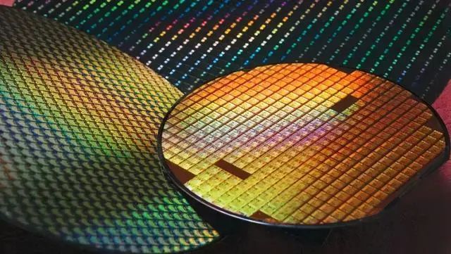
II. Basic Concepts
The core concept of photolithography is to transfer the precise pattern onto the photosensitive layer on the surface of a silicon wafer through optical projection, and then create the desired micro-pattern on the wafer through chemical processing. In this section, we will explain in detail the basic principles and steps of photolithography, as well as the main functions and components of photolithography machines.
2.1 Basic Principles
The basic principles of photolithography involve the following key concepts:
Photomask: One of the important elements that controls the final pattern. The photomask is a flat glass or quartz plate with a pattern that is blocked or transmitted through the photoresist during photolithography. This pattern is created using computer-aided design (CAD) software and is used for projection in photolithography.
Light source: One of the key parts of the photolithography machine. Usually, ultraviolet (UV) light sources are used because of their shorter wavelength, which enables higher resolution. The UV light source is irradiated onto the photomask and then the pattern is projected onto the surface of the silicon wafer through a series of lenses and reflectors.
Photosensitive layer: The goal of photolithography is to replicate the pattern on the photomask onto the silicon wafer. To achieve this, the silicon wafer needs to be covered with a layer of photosensitive material, typically photoresist. The photosensitive layer can be chemically altered by the irradiation of the light source on the photolithography machine.
2.2 Steps of Photolithography
The steps of photolithography usually include the following:
Wafer preparation: First, the silicon wafer is prepared, typically through chemical cleaning and other pre-treatment steps, to ensure the success of photolithography.
Photoresist coating: The photoresist is evenly coated on the surface of the silicon wafer. The photoresist is part of the photosensitive layer and is used to receive the projection of light and undergo chemical reactions in subsequent steps.
Mask alignment: The photolithography machine ensures that the mask and the silicon wafer are aligned so that the pattern can be accurately projected onto the silicon wafer.
Light projection: The light source projects the pattern on the photomask precisely onto the photosensitive layer. The photosensitive layer undergoes a chemical reaction under the irradiation of light, and its properties change.
Photoresist development: Next, the silicon wafer is placed into a special solution called the developing solution. The developing solution removes the photoresist that has not been irradiated by light, leaving only the irradiated part to form the desired pattern.
Post-processing: Depending on specific application requirements, the silicon wafer may need further chemical or physical processing steps, such as etching, ion implantation, or metal deposition.
Repeating and combining these steps allows for the creation of complex micro-circuit patterns on the silicon wafer, which constitute the core components of modern electronic devices.
The key function of the photolithography machine is to control the interaction between the light source, photomask, and photosensitive layer to achieve precise pattern transfer. The choice and preparation of photomasks, the stability of the light source, and the performance of the photoresist all have a significant impact on the quality and resolution of the final pattern. Accurate alignment and the performance of the optical system are also critical factors to ensure success. The precision and complexity of photolithography make it an indispensable part of semiconductor manufacturing.
III. Historical Review
3.1 The Origins and Development of Early Photolithography Technology
The history of photolithography can be traced back to the 19th century, where early photographic techniques provided crucial inspiration for future semiconductor manufacturing. Here are some important stages in the early development of photolithography:
Inspiration from Early Photography (19th Century)
In the mid-19th century, the rise of photography laid the foundation for photolithography. One of the earliest photographic methods was the silver salt process, which used photosensitive silver salts to capture images when exposed to light. This inspired scientists to explore the application of photosensitive materials in semiconductor manufacturing.
Early Attempts at Photolithography in Semiconductor Manufacturing (Early 20th Century)
In the early 20th century, scientists began experimenting with applying photolithography techniques to semiconductor manufacturing. However, the technological limitations at the time restricted resolution and precision, making the fabrication of microcircuits highly limited.
Contributions from Michelson Interferometer (Early 20th Century)
In the early 20th century, Albert A. Michelson invented the interferometer, an instrument used to measure the wavelength of light. This discovery had a profound impact on the precision and resolution of photolithography, making it possible to create finer patterns.
3.2 The Key Role of Photolithography in the Semiconductor Industry Revolution
Photolithography played a crucial role in the semiconductor industry revolution, driving the rapid advancement of electronic technology. Here are key contributions of photolithography during this historical period:
Birth of Integrated Circuits (1950s)
In the 1950s, the invention of the first transistor marked the beginning of the era of integrated circuits. Photolithography became a critical step in accurately fabricating circuit patterns on silicon wafers, enabling millions or even billions of transistors to be integrated on a single chip, greatly enhancing computer performance.
Supporting Moore's Law (1965)
In 1965, Gordon Moore, co-founder of Intel Corporation, proposed Moore's Law, which predicted the exponential growth of transistors on integrated circuits. The continuous improvement and innovation in photolithography enabled the realization of this law, driving rapid advancements in the semiconductor industry.
Rapid Development of Electronic Devices (Late 20th Century to Present)
The continuous evolution of photolithography has made electronic devices smaller, faster, and more powerful, such as smartphones, computers, tablets, and various embedded systems. These devices have profoundly transformed our daily lives and fueled innovations in communication, healthcare, entertainment, and scientific fields.
In conclusion, the origins and development of photolithography are integral to the semiconductor industry revolution. Its advancements not only propelled the rapid progress of electronic technology but also brought countless opportunities and transformations to modern science and society. As technology continues to advance, photolithography remains a critical step in electronic manufacturing and will continue to drive technological advancements in the future.
To be continued...



Site Map | 萨科微 | 金航标 | Slkor | Kinghelm
RU | FR | DE | IT | ES | PT | JA | KO | AR | TR | TH | MS | VI | MG | FA | ZH-TW | HR | BG | SD| GD | SN | SM | PS | LB | KY | KU | HAW | CO | AM | UZ | TG | SU | ST | ML | KK | NY | ZU | YO | TE | TA | SO| PA| NE | MN | MI | LA | LO | KM | KN
| JW | IG | HMN | HA | EO | CEB | BS | BN | UR | HT | KA | EU | AZ | HY | YI |MK | IS | BE | CY | GA | SW | SV | AF | FA | TR | TH | MT | HU | GL | ET | NL | DA | CS | FI | EL | HI | NO | PL | RO | CA | TL | IW | LV | ID | LT | SR | SQ | SL | UK
Copyright ©2015-2025 Shenzhen Slkor Micro Semicon Co., Ltd