In the semiconductor industry, photolithography technology serves as the cornerstone for chip manufacturing, governing the structure and performance of chips. It allows us to fabricate circuit structures at the micro or even nanometer scale, making it a vital component of various electronic devices. Each generation of chip manufacturing relies on the innovation of photolithography technology, as it determines the expansion of chip functionality and performance enhancement.
Photolithography machines have undergone five generations of product development, with each improvement and innovation significantly enhancing the smallest achievable process node of the machines. Progressing from light sources such as g-line and i-line to KrF, ArF, and EUV, and evolving in operational principles from contact proximity lithography machines to immersion stepper projection lithography machines and extreme ultraviolet lithography machines.
In the 1960s, contact lithography technology emerged as the primary photolithography technique during the era of small-scale integrated circuits. In contact lithography, the mask aligns directly with the wafer's photosensitive surface, exposing the entire substrate in one go. The size relationship between the mask pattern and wafer pattern is 1:1, achieving submicron-level resolution. Contact lithography minimizes light diffraction effects, but the direct contact between the wafer and mask during exposure can lead to friction-induced scratches, particle contamination, reduced wafer yield, and decreased mask longevity, necessitating frequent mask replacements. Hence, proximity lithography technology was introduced.
During the 1970s, proximity lithography technology gained widespread use. Unlike contact lithography, proximity lithography involves a gap filled with nitrogen gas between the mask and wafer surface, without direct contact. The minimum resolution size is proportional to the gap, with higher resolutions achieved with smaller gaps. However, the distance between the mask and wafer causes diffraction effects, limiting the spatial resolution of proximity lithography machines to around 2μm. As feature sizes decreased, projection lithography technology emerged.
In the mid to late 1970s, projection lithography technology based on far-field Fourier optical imaging principles introduced a projection imaging lens with magnification between the mask and photoresist, significantly enhancing resolution. Initially, the mask-to-substrate pattern size ratio was 1:1.
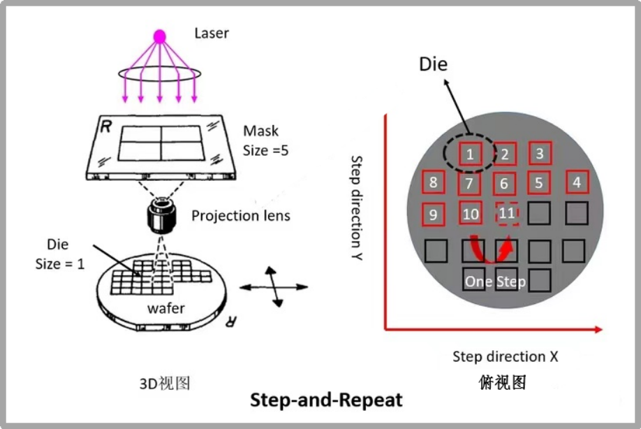
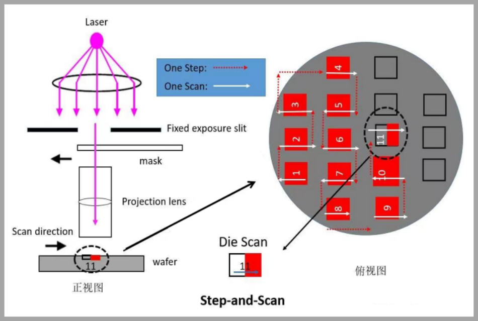
As integrated circuit sizes continue to shrink, step-and-repeat lithography technology with reduction ratios has emerged. In step-and-repeat lithography, the mask remains stationary while the wafer moves incrementally to complete the entire exposure process. With the increasing integration level of integrated circuits and the expansion of chip areas, there is a demand for larger exposure areas in a single shot, leading to the advent of more advanced step-and-scan lithography machines. Currently, step-and-repeat lithography is primarily applied in processes above 0.25μm and in advanced packaging fields. Step-and-scan lithography technology offers advantages in exposure field size and uniformity, reducing the need for step-and-repeat lithography machines in manufacturing below 0.25μm.
Step-and-scan lithography employs a dynamic scanning method where the mask synchronously scans with the wafer to the next exposure field position after each exposure, continuing the repetitive exposure process until the entire wafer is exposed. Starting from the 0.18μm node, step-and-scan lithography has been widely adopted in silicon-based CMOS processes, and for processes below 7nm, EUV lithography also utilizes the step-and-scan approach.
Projection lithography technology can be divided into dry lithography and immersion lithography based on whether there is water as a medium between the projection lens and the wafer.
Dry lithography technology cannot meet the requirements of continuously shrinking linewidths: When light exits the projection lens and enters the air medium from the glass medium, diffraction occurs. This causes changes in the light angle, resulting in the final image formation on the wafer surface. As the linewidth decreases, the diffraction effect increases, requiring larger projection lens diameters to capture more light. This leads to an increasing convergence angle of the light within the lens. After refraction, the light angle exiting the projection lens becomes nearly horizontal, making it impossible to achieve imaging. Therefore, immersion lithography technology was developed.
Immersion lithography technology further enhances the capabilities of lithography: The space between the projection lens and the wafer is filled with water. Due to the similarity in refractive indices between water and glass (at a wavelength of 193nm, the refractive index of air is 1, water is 1.44, and glass is approximately 1.5), when light emitted from the projection lens enters the water medium, the refraction angle becomes smaller. This allows the light to refract properly out of the lens. With the addition of immersion technology, the actual effective wavelength of ArF light source is 193nm/1.44=134nm.
Lithography technology utilizes multiple exposure techniques to achieve smaller linewidths. Three common multiple exposure techniques are LELE (LITHO-ETCH-LITHO-ETCH), LFLE (LITHO-FILM-LITHO-ETCH), and SADP (SELF-ALIGNED DOUBLE PATTERNING). Among them, SADP has smaller errors.
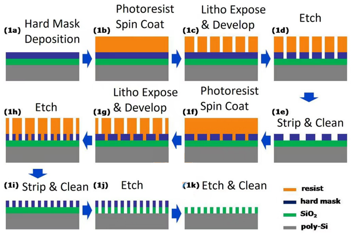
1) LELE (LITHO-ETCH-LITHO-ETCH): This technique involves splitting the original lithographic pattern onto two or more masks, using multiple exposures and etching steps to achieve the desired design.
The process flowchart for LELE lithography technology
2) LFLE (LITHO-FREEZE-LITHO-ETCH): This technique involves applying a second layer of photoresist on top of the first layer that has been chemically frozen but not removed. Subsequent lithography is carried out to form a dual structure. The key characteristics of LELE and LFLE technologies are their simple processes, but they suffer from alignment issues between the two lithography steps. If the process is not rigorous enough, deviations in linewidth between each exposure and overlay errors between the two exposure patterns can lead to localized periodic variations in the patterns.
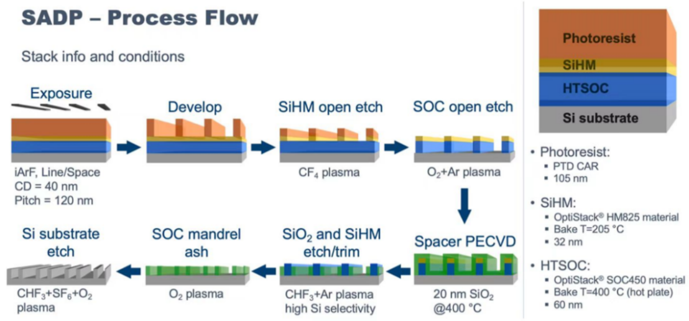
3) SADP, also known as Self-Aligned Double Patterning, utilizes deposition and etching techniques to enhance lithographic precision. A metal medium layer, hard mask material, and sacrificial layer (core axis material) are deposited on the wafer, followed by the spinning of a photoresist. After exposure and development, the desired pattern is left behind, and the core axis is etched. Then, an additional sidewall is deposited around the core axis periphery, where the size of the sidewall determines the pitch of the interconnect lines. Precise control of uniformity is essential to ensure the consistency of the pitch. The core axis material is removed, leaving only the sidewalls. Subsequent etching transfers the sidewall pattern to the underlying mask layer. After removing the sidewalls and modifying the mask layer, the pattern is transferred to the metal medium layer after another etching step, resulting in a final pattern with a linewidth only half of the original. SADP can achieve up to four times the precision in two steps.
Multiple exposure can achieve a 7nm process, but the technology is complex and costly: Multiple iterations of LE or SADP can achieve a 7nm process, but the increased technical requirements for etching, deposition, and the higher number of usage cycles have doubled or tripled the cost of wafer lithography.
With the development of micro-nano fabrication technology, the field of lithography has been expanding beyond contact, projection, scanning, and step-and-repeat lithography techniques.
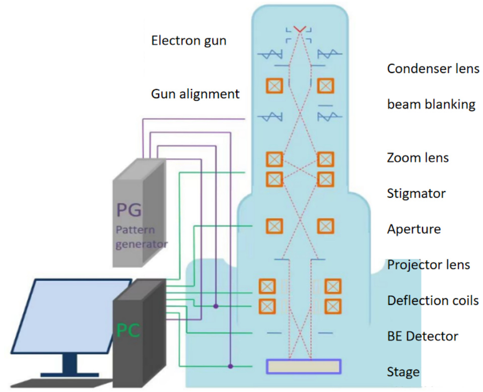
Electron beam lithography (EBL) systems are devices that generate and control a focused electron beam to directly write patterns according to the design layout. In basic principles, EBL is similar to scanning electron microscopy. It consists of a beam column (which generates and controls the focused electron beam), an electron beam detection system (which detects the intensity of the electron beam reaching the sample surface), a reflected electron detection system (which observes alignment markers on the sample surface), a stage system (which holds and precisely moves the sample), a vacuum system (which provides a high vacuum environment), and a high-voltage power supply and computer graphics system (which converts the design data into electric signals to control the deflection of the electron beam). Electron beam lithography systems have various applications and are important tools for obtaining nanoscale patterns. They are widely used in research fields such as new materials (e.g., metamaterials, surface engineering), cutting-edge physics (e.g., superconductivity, quantum phenomena), biomimetics (functional surfaces), photonics (micro/nano optics, waveguides, photonic crystals), biology (DNA analysis, nanofluidics), and microelectronics. In recent years, with the development of the technology market, electron beam lithography has also been utilized in the fabrication of 3D structured optical devices, photonics chip fabrication, high-power chip fabrication, and traditional mask production.

Schematic diagram of an electron beam exposure system
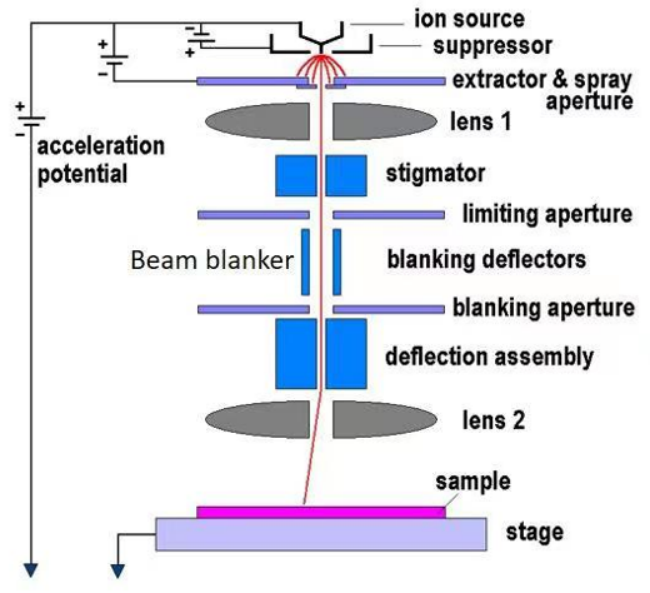
Ion beam lithography: Ion beams, similar to electron beams, are focused charged particles formed through electromagnetic fields. The main difference between them lies in their mass. Clearly, ions have a much higher mass than electrons, which effectively avoids the problem of electron beam scattering. Ion beam lithography can achieve higher resolution than electron beam lithography, with a minimum resolution reaching 5nm. Ion beams have high sensitivity, which is both an advantage and a disadvantage. The high sensitivity requires a relatively small number of ions, leading to significant statistical noise and increased random fluctuations, resulting in increased roughness at the edges of the exposed patterns. However, ion beam exposure faces challenges such as limited penetration depth, even for gallium ion beams with 100keV energy, the exposure depth is less than 0.1μm. Additionally, the complexity and high cost of ion beam exposure systems and processes have hindered its development.
Due to the ability of heavy ion beams to directly remove atoms from solid surfaces, focused ion beams are more widely used as direct microfabrication tools, such as ion sputtering and ion beam-assisted deposition. Especially in the production and development of semiconductor integrated circuits, focused ion beams play a crucial role. Their major applications include circuit inspection and modification, repairing defects in photomasks, fabricating transmission electron microscope samples, ion implantation for altering the conductivity of semiconductor materials, and serving as a versatile cutting tool, among others.
Schematic diagram of a focused ion beam exposure device
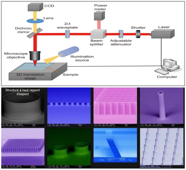
Laser direct writing lithography involves varying the intensity of a laser beam to selectively expose the resist material on a substrate, forming the desired relief contour on the resist layer after development. The basic working principle of a laser direct writing system is to control a high-precision laser beam scan using a computer, directly exposing the designed pattern on the photoresist to transfer the design onto a mask. The laser direct writing system mainly consists of a He-Cd laser, acousto-optic modulator, projection lithography objective lens, CCD camera, display monitor, illumination source, worktable, focusing device, He-Ne laser interferometer, and control computer. The basic workflow of laser direct writing includes generating micro-optical elements or VLSI mask structure data on a computer, converting the data into control data for the direct writing system, scanning and exposing the photoresist with a high-precision laser beam controlled by the computer, and transferring the designed pattern onto the substrate through development and etching.
Laser direct writing lithography is limited by the laser wavelength and does not offer the same lithographic precision as charged particle lithography techniques like electron beams and ion beams. As a result, it may not meet the requirements of advanced semiconductor device manufacturing but finds more applications in the photovoltaic field. Currently, laser direct writing is gaining widespread attention and application, particularly in the field of photovoltaic electroplating copper.
Schematic diagram and results display of laser direct writing lithography
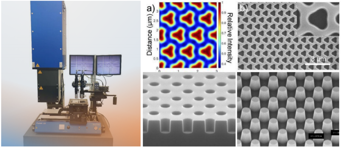
The grating exposure system is a low-cost optical exposure system capable of achieving high-resolution periodic structures. Similar to traditional UV exposure machines, a substrate coated with photoresist is placed beneath a mask in a non-contact manner and exposed to ultraviolet light. Thanks to Displacement Talbot Lithography (DTL) technology, high-resolution pattern exposure can be achieved without the need for complex optical path systems. This technology overcomes the diffraction limitations of traditional lithography, resulting in superior exposure quality for submicron to nanoscale periodic patterns. During the exposure process, the mask and substrate remain non-contact, thereby avoiding contamination or damage to the mask.
DTL technology utilizes the principle of optical diffraction self-imaging to break through the traditional exposure accuracy limits, with no depth of field restrictions and no need for focusing during exposure. This allows the lithography machine to achieve high uniformity patterns even on non-planar surfaces or thicker photoresists. However, the grating exposure system is not suitable for all types of patterns and is primarily designed for periodic or quasi-periodic patterns. Its main applications include XR (AR/VR/MR), optoelectronic devices, optical devices, and biomedicine.

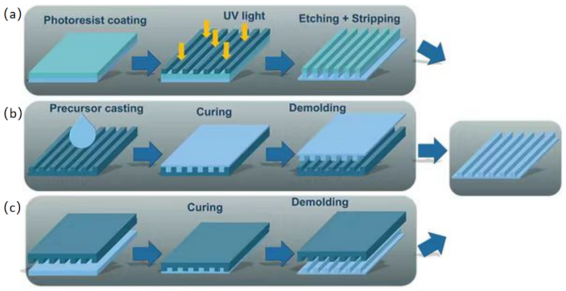
Nanoimprint lithography (NIL) is a micro-nanofabrication technique that involves transferring tiny patterns designed and fabricated on a template onto a polymer-coated substrate through imprinting. The resolution of imprinting is determined by the structure size of the template pattern, without the diffraction limits present in the projection optical systems of photolithography machines. This technology enables the replication of nanoscale linewidth patterns and structures. NIL does not require complex optical systems or expensive light sources, leading to significant cost reduction in manufacturing. With NIL, as long as the pattern is pre-fabricated, even complex structures can be formed in a single step. However, NIL technology currently faces challenges such as template defects and alignment accuracy, which need time to be resolved before it can maturely enter the market.

In conclusion, from its inception to the present, the lithography machine has undergone multiple iterations and has developed various application technologies. In order to meet the ever-evolving application demands, new technological peaks and challenges are also waiting for the industry to climb and overcome."

