Service hotline
+86 0755-83044319
release time:2023-10-11Author source:SlkorBrowse:8591
In previous articles, we introduced wafer fabrication, oxidation processes, and a partial history of integrated circuits. Now, let's continue to explore the photolithography process, which transfers the electronic circuit patterns onto the wafer. Photolithography is similar to taking photographs with a film camera, but how does it work exactly?
Photolithography, similar to developing black and white photos
Photolithography, commonly referred to as "photo," is named for its process of transferring circuit designs onto wafers by exposing the patterns through a photomask. Creating replicas on wafers is similar to developing black and white films on photosensitive paper.
As circuit patterns become increasingly dense, chip components also need to be reduced using high-precision nanoscale processes. Producing these finer circuit patterns relies heavily on the photolithography process. Therefore, as chips shrink in size, high precision and advanced photolithography technology are essential.
Preparing to draw circuit patterns on wafers
Let's take a closer look at the photolithography process. The first step is to use computer-aided design software (EDA) to design the circuit patterns to be drawn on the wafer. On the canvas of this electronic circuit pattern, engineers will create a precisely designed layout that determines the integration level of the semiconductor chip.
Creating photomasks that function similarly to photographic negatives
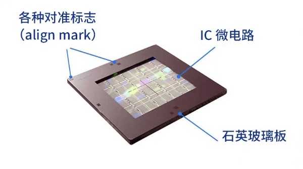
Using chromium (Cr), the microcircuits are transferred onto a glass substrate made of ultra-pure quartz to create the photomask that represents the circuit design. The photomask, also known as a reticle, functions like photographic film, reflecting the circuit patterns. In order to achieve finer patterns, the photomask is designed to be much larger than the circuit dimensions and then optically shrunk onto the wafer using lens optics.
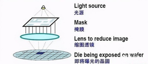
The photolithography process includes coating, exposure, and development stages.
1. Coating: A layer of photoresist (PR) is coated onto the surface of the wafer.
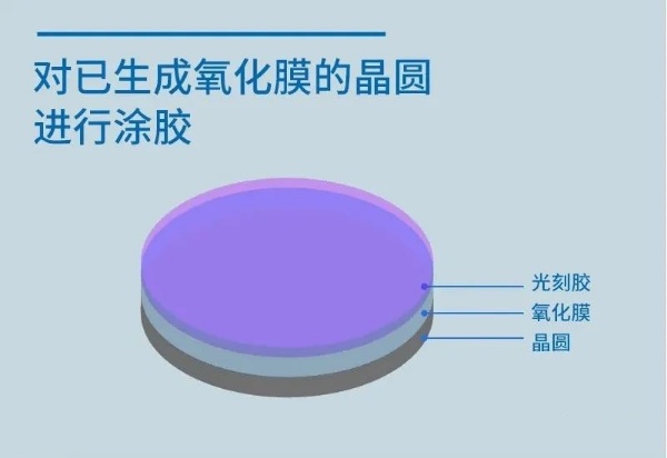
With the preparation complete, the next step is to draw patterns on the wafer. First, a layer of photoresist (PR) that is sensitive to light is evenly applied onto the surface of the wafer. This makes the wafer act as photosensitive paper used in developing photos. The photoresist layer needs to be thin and uniform, as well as highly sensitive to ultraviolet light to produce high-quality and precise circuit patterns.
2. Exposure: The circuit patterns are drawn on the wafer using light.
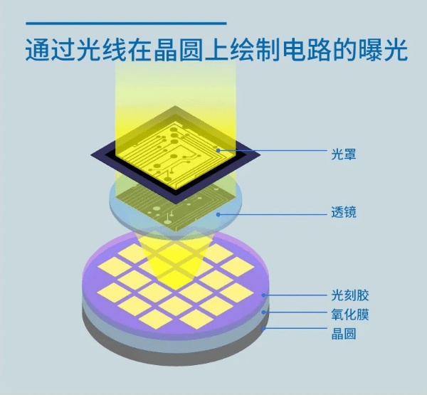
By using a stepper, the circuit design on the photomask is projected and transferred onto the wafer coated with photoresist using ultraviolet light. This process is called "step-and-repeat exposure." Due to the high precision required for semiconductor chips, the exposure area is selectable and precisely controlled.
3. Development: Circuit patterns are formed through the development process.
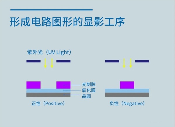
The last step of the photolithography process is called development, which is similar to the process of developing a photograph. This step is crucial as it determines the final shape of the circuit patterns on the wafer. As the developer solution is sprayed onto the wafer, selective removal of certain areas occurs to create the desired pattern.
The photoresist can be either positive or negative, depending on its reaction to light. If a positive photoresist is used, the areas exposed to light (exposed) are removed during development, leaving behind the unexposed areas. Conversely, if a negative photoresist is used, the opposite occurs.
Once the development step is completed, the photolithography process is finished. Various instruments, including optical microscopes, are used to carefully inspect the wafer. Only wafers that pass all inspections proceed to the next step.
In this article, we have introduced the photolithography process, which involves projecting precise circuit designs onto the wafer. Stay tuned for the next part of this series, where we will learn how to selectively remove unnecessary materials through the etching process to create the desired circuit patterns on the wafer.



Site Map | 萨科微 | 金航标 | Slkor | Kinghelm
RU | FR | DE | IT | ES | PT | JA | KO | AR | TR | TH | MS | VI | MG | FA | ZH-TW | HR | BG | SD| GD | SN | SM | PS | LB | KY | KU | HAW | CO | AM | UZ | TG | SU | ST | ML | KK | NY | ZU | YO | TE | TA | SO| PA| NE | MN | MI | LA | LO | KM | KN
| JW | IG | HMN | HA | EO | CEB | BS | BN | UR | HT | KA | EU | AZ | HY | YI |MK | IS | BE | CY | GA | SW | SV | AF | FA | TR | TH | MT | HU | GL | ET | NL | DA | CS | FI | EL | HI | NO | PL | RO | CA | TL | IW | LV | ID | LT | SR | SQ | SL | UK
Copyright ©2015-2025 Shenzhen Slkor Micro Semicon Co., Ltd