Service hotline
+86 0755-83044319
release time:2023-10-12Author source:SlkorBrowse:8881
Semiconductor chips are composed of many microscale layers that are smaller than a fingernail and thinner than paper. The semiconductor is stacked high and dense, forming complex structures similar to high-rise buildings.
To create such structures, the following steps need to be repeated multiple times: lithography - coating the top of a single-crystal silicon wafer (the raw material for semiconductors) with a thin film and patterning circuits, etching - selectively removing unnecessary materials, and then cleaning the surface impurities.
After the etching and cleaning processes, the thin film functions to separate, connect, and protect the circuits. Next, we will introduce the deposition process for manufacturing thin films and the ion implantation process for imparting semiconductor electrical properties.
Deposition process: applying thin films to the wafer
The term "thin film" refers to a film that is 1 micron (μm) or thinner, a thickness that cannot be achieved through simple mechanical processing. Deposition is a series of processes that involve coating the wafer with the desired molecular or atomic level thin films. Due to the extremely thin nature of the films, precise techniques are required to uniformly apply the films onto the wafer.
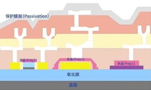
Deposition can generally be divided into two types. These two types are Physical Vapor Deposition (PVD) and Chemical Vapor Deposition (CVD).
Physical Vapor Deposition is mainly used for depositing metal films without involving chemical reactions. On the other hand, Chemical Vapor Deposition involves applying external energy to particle vapor formed by gas chemical reactions, and the vapor is sprayed onto the surface for deposition. This technique can be used to deposit thin films onto conductors, insulators, and semiconductors.
Chemical Vapor Deposition is the most widely used deposition method in current semiconductor processes. It can further be classified into Thermal CVD, Plasma CVD, and Photo-induced CVD, depending on the external energy source used. Among these, Plasma CVD is the most common application as it can form films at low temperatures, control film thickness uniformity, and handle high volumes.
The thin film formed through the deposition process consists of two layers: a metallic (conductive) layer for connecting electrical signals between circuits, and an insulating layer for electrical isolation between internal interconnect layers or preventing contaminants from entering.
Ion implantation: transforming wafers into semiconductors.

At this point, a process is still needed to impart electrical characteristics to the semiconductor. Semiconductors possess both conductor and insulator properties, and ion implantation is the process of essentially transforming silicon wafers into semiconductors. Pure silicon is an insulator and does not conduct electricity, but the addition of impurities imparts conductivity, enabling it to carry electrical currents.
These impurities are known as ions. These ions are converted into tiny gas-like particles and then implanted into the front side of the wafer to the desired depth. The impurities used come from the 15th group (P, phosphorus; As, arsenic) or the 13th group (B, boron) of the periodic table. Implanting elements from the 15th group results in an n-type semiconductor (electron-type), while implanting elements from the 13th group results in a p-type semiconductor (hole-type).
The deposition process is crucial because the thickness and uniformity of the deposited films determine the quality of the semiconductor. The thickness of future semiconductor circuit structures will be millions of times thinner than a human hair. In order for these circuits to have electrical properties, more advanced deposition techniques are required to generate thinner and more uniform thin films.
In the next article, we will learn about metal interconnects, which aim to connect the elements generated through oxidation, photolithography, etching, and deposition processes and form circuits.



Site Map | 萨科微 | 金航标 | Slkor | Kinghelm
RU | FR | DE | IT | ES | PT | JA | KO | AR | TR | TH | MS | VI | MG | FA | ZH-TW | HR | BG | SD| GD | SN | SM | PS | LB | KY | KU | HAW | CO | AM | UZ | TG | SU | ST | ML | KK | NY | ZU | YO | TE | TA | SO| PA| NE | MN | MI | LA | LO | KM | KN
| JW | IG | HMN | HA | EO | CEB | BS | BN | UR | HT | KA | EU | AZ | HY | YI |MK | IS | BE | CY | GA | SW | SV | AF | FA | TR | TH | MT | HU | GL | ET | NL | DA | CS | FI | EL | HI | NO | PL | RO | CA | TL | IW | LV | ID | LT | SR | SQ | SL | UK
Copyright ©2015-2025 Shenzhen Slkor Micro Semicon Co., Ltd