Service hotline
+86 0755-83044319
release time:2023-10-12Author source:SlkorBrowse:8576
Semiconductors possess both "conductor" properties, allowing electric currents to pass through, and "insulator" properties, which do not allow electric currents to pass. The ion implantation process adds impurities to pure silicon to give it conductivity. We can make the semiconductor conductive or insulating depending on our needs.
Repeating the photolithography, etching, and ion implantation steps creates countless semiconductor circuits on the wafer. External electrical signals must be applied for these circuits to function properly. Metal interconnects are laid out along the semiconductor circuit design to facilitate the transmission of electrical signals through the circuit.
Metal interconnects: Laying out electrical highways
The metal interconnect process is designed to take advantage of the conducting properties of metals. In this step, metal wires are deposited according to the semiconductor circuit design pattern. However, not all metals can be used for metal interconnects. To improve the quality of the semiconductor chip, metals must satisfy the following conditions:
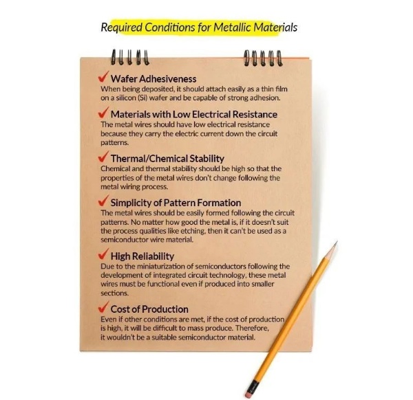
- When deposited, it is easy to form a thin film on the wafer and has strong adhesion.
- Low impedance to reduce losses.
- High chemical and thermal stability to ensure stable electrical characteristics.
- Easy formation of circuit patterns suitable for etching and other processes.
- High reliability even at extremely small sizes.
- Low cost to meet the demands of large-scale production.
Metals that meet the above conditions include aluminum (Al), titanium (Ti), and tungsten (W). So how is metal interconnect formed?
.jpg)
Aluminum is the most common material used in the metal interconnect process of semiconductor chips because it adheres well to the oxide layer (silicon dioxide) and is easy to process. However, when aluminum (Al) and silicon (Si) come into contact, they often mix. This means that when laying aluminum wires on a silicon wafer, the junction surface may be compromised. To prevent this from happening, another metal is deposited as a barrier between the aluminum and the wafer. This metal is called a barrier metal. By forming a double-layered thin film, the junction surface can be protected from being destroyed.
Metal wire laying uses a deposition process. The metal is placed in a vacuum chamber and boiled or electrified at low pressure to turn it into gas. The wafer is then placed in the vacuum chamber, allowing a thin metal film to form on the wafer.
Through continuous research and development, semiconductor processes are becoming increasingly sophisticated. For example, the metal interconnect process is transitioning to chemical vapor deposition (CVD) to form more uniform thin films in smaller areas.
We have studied the processes involved in wafer manufacturing, circuit schematic design, and semiconductor chip creation. Next, we will examine the final steps in the journey to producing a perfect semiconductor product: testing and packaging.



Site Map | 萨科微 | 金航标 | Slkor | Kinghelm
RU | FR | DE | IT | ES | PT | JA | KO | AR | TR | TH | MS | VI | MG | FA | ZH-TW | HR | BG | SD| GD | SN | SM | PS | LB | KY | KU | HAW | CO | AM | UZ | TG | SU | ST | ML | KK | NY | ZU | YO | TE | TA | SO| PA| NE | MN | MI | LA | LO | KM | KN
| JW | IG | HMN | HA | EO | CEB | BS | BN | UR | HT | KA | EU | AZ | HY | YI |MK | IS | BE | CY | GA | SW | SV | AF | FA | TR | TH | MT | HU | GL | ET | NL | DA | CS | FI | EL | HI | NO | PL | RO | CA | TL | IW | LV | ID | LT | SR | SQ | SL | UK
Copyright ©2015-2025 Shenzhen Slkor Micro Semicon Co., Ltd