Service hotline
+86 0755-83044319
release time:2023-10-11Author source:SlkorBrowse:8825
Semiconductors have become an essential part of our lives. Today, we return to the "Eight Basic Semiconductor Processes" series to continue exploring semiconductor manufacturing processes. In the previous article, we learned about the wafer manufacturing process. In this article, we will introduce the oxidation process.
Wafer Oxide Layer (Silicon Dioxide, SiO2): Provides protection and insulation.

Before being used as raw materials for integrated circuits, silicon extracted from sand undergoes a series of purification processes to form a silicon ingot. The silicon ingot is then sliced into uniform thickness, polished, and eventually formed into the foundation of semiconductor-wafers.
The wafers produced from these steps are not conductive. Therefore, further processing is required to make them "semiconductor", with both conductive and non-conductive properties. To achieve this, various substances need to be transferred onto the wafer, and circuit patterns are etched onto the surface. These processes may need to be repeated multiple times.

Oxidation is the basis of all the processes mentioned above. The oxidation process produces a layer of SiO2, which is used as an insulating layer to prevent leakage current between circuits. The oxide layer can also protect the silicon wafer during subsequent ion implantation and etching processes.
In other words, the silicon dioxide layer acts as a reliable shielding layer throughout the semiconductor manufacturing process. Integrated circuits require high precision, and even tiny contaminants can have adverse effects on the electrical performance of the integrated circuit, making the role of the oxide layer crucial.
How is this protective oxide layer formed?
When the wafer is exposed to oxygen in the air or other chemical substances, it forms an oxide layer, similar to how iron (Fe) rusts when exposed to air.
There are several methods of oxidation, such as thermal oxidation, plasma-enhanced chemical vapor deposition (PECVD), and electrochemical anodization. Among them, the most widely used is the thermal oxidation process conducted at high temperatures of 800-1200°C to form a thin and uniform layer of silicon dioxide.
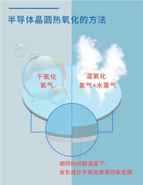
Thermal oxidation can be classified into dry oxidation and wet oxidation, depending on the gases used for the oxidation reaction. Dry oxidation uses pure oxygen (O₂), resulting in slower growth of the oxide layer, making it an ideal choice for forming thin layers. Oxides produced through the dry method exhibit excellent electrical characteristics. Wet oxidation employs both oxygen (O₂) and water vapor (H₂O). As a result, the oxide layer grows faster and becomes thicker. However, oxides produced through the wet method are not as dense as those formed through the dry method. Under the same time and temperature conditions, the oxide formed through the wet method is approximately five to ten times thicker than the one formed through the dry method.
This article primarily introduces the function of oxide layers and how they are formed. Please stay tuned for the next part of this series, where we will explain how circuit patterns are printed on wafers covered with oxide layers.



Site Map | 萨科微 | 金航标 | Slkor | Kinghelm
RU | FR | DE | IT | ES | PT | JA | KO | AR | TR | TH | MS | VI | MG | FA | ZH-TW | HR | BG | SD| GD | SN | SM | PS | LB | KY | KU | HAW | CO | AM | UZ | TG | SU | ST | ML | KK | NY | ZU | YO | TE | TA | SO| PA| NE | MN | MI | LA | LO | KM | KN
| JW | IG | HMN | HA | EO | CEB | BS | BN | UR | HT | KA | EU | AZ | HY | YI |MK | IS | BE | CY | GA | SW | SV | AF | FA | TR | TH | MT | HU | GL | ET | NL | DA | CS | FI | EL | HI | NO | PL | RO | CA | TL | IW | LV | ID | LT | SR | SQ | SL | UK
Copyright ©2015-2025 Shenzhen Slkor Micro Semicon Co., Ltd