Service hotline
+86 0755-83044319
release time:2023-10-11Author source:SlkorBrowse:15228
In the previous article, we introduced the photolithography process, which uses a photomask to project the designed circuit patterns onto the surface of the wafer coated with photoresist. The next step is to perform the etching process on the wafer to remove unwanted material and retain only the desired pattern.
Etching: An Art Form in Its Own Right
When you were in art classes, you may have created "prints," a type of artwork created by drawing shapes on the surface of wood, metal, or stone, then applying ink or paint and pressing it onto paper or fabric. The semiconductor etching process shares similar principles with this printmaking technique.
In printmaking, an anti-corrosive material is applied to a metal plate, and the desired design is carved into the plate using sharp tools. The plate is then immersed in corrosive materials such as nitric acid, and the degree of corrosion is controlled to form the desired pattern.
Similarly, in semiconductor manufacturing, the etching process uses liquid or gas etchants to selectively remove unwanted materials until the desired circuit patterns are left on the surface of the wafer. The material in areas without photoresist is removed by the etchant to form the circuit patterns on the wafer. After the etching process is complete, the photoresist is removed. These steps need to be repeated multiple times on different layers.

Dry etching, used in the etching process, can be classified into two types: dry etching and wet etching, depending on the materials used. Dry etching selectively removes unwanted materials using reactive gases and ions, while wet etching uses chemical solutions.
Compared to wet etching, dry etching has higher costs and is more complex. However, with the advancement of nanoscale semiconductor technology, circuits are becoming more finely complex. Therefore, dry etching is more widely applied and has a higher yield (referring to the percentage of finished products).
Dry etching, also known as plasma etching, is used to remove unnecessary substrate materials.
Plasma is generated by injecting gas into a vacuum chamber at a pressure lower than atmospheric pressure and then providing electrical energy. Plasma is a state of matter (similar to solids, liquids, and gases) composed of a large number of free electrons, ions, and neutral particles or ionized gases. When a substance is ionized, it means that neutrons or molecules have changed their charge state by losing or gaining electrons.
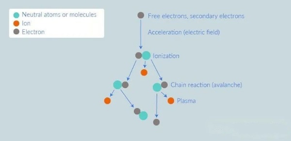
When a sufficiently strong magnetic field generated by electrical energy is applied to a gas, causing the gas molecules to collide and ionize, a plasma is formed. In other words, free electrons are accelerated by the magnetic field, and the subsequent high-energy electrons collide with neutrons or molecules, ionizing them.
This ionization cascade, known as the avalanche effect, leads to an exponential increase in the number of ions. This is what we call the "plasma state." Free radical atoms dissociate from this plasma state and evaporate away from the wafer surface, thereby removing the surface material that was previously unprotected by the photoresist coating.
There are several points to note in the dry etching process.
First, uniformity. Uniformity indicates the consistency of the etching rate across the entire wafer surface. If the etching rate is inconsistent in different areas of the wafer, the etch depth will vary, which could lead to chip failures.
Second, etch rate. This refers to the amount of surface material removed in a given time. The etch rate can vary depending on the number of reactive atoms and ions, as well as the energy carried by the ions that cause surface reactions to occur. In other words, we need to strictly control these factors to improve overall yield.
In addition, selectivity (the ratio of the etch rate of the target material to the etch rate of other materials) and etch profile are also considered important factors in dry etching.
Now you have a better understanding of the etching process for constructing semiconductor circuit patterns. Semiconductors are the epitome of integrated circuit technology, manufactured through the repeated deposition of desired materials onto a silicon substrate, application of protective layers, and selective etching of unnecessary parts. The entire process is carried out in instruments designed with safety in mind.
In the next article, we will introduce the deposition and ion implantation processes, which impart electrical properties to wafers through these techniques.



Site Map | 萨科微 | 金航标 | Slkor | Kinghelm
RU | FR | DE | IT | ES | PT | JA | KO | AR | TR | TH | MS | VI | MG | FA | ZH-TW | HR | BG | SD| GD | SN | SM | PS | LB | KY | KU | HAW | CO | AM | UZ | TG | SU | ST | ML | KK | NY | ZU | YO | TE | TA | SO| PA| NE | MN | MI | LA | LO | KM | KN
| JW | IG | HMN | HA | EO | CEB | BS | BN | UR | HT | KA | EU | AZ | HY | YI |MK | IS | BE | CY | GA | SW | SV | AF | FA | TR | TH | MT | HU | GL | ET | NL | DA | CS | FI | EL | HI | NO | PL | RO | CA | TL | IW | LV | ID | LT | SR | SQ | SL | UK
Copyright ©2015-2025 Shenzhen Slkor Micro Semicon Co., Ltd