Service hotline
+86 0755-83044319
release time:2023-09-09Author source:SlkorBrowse:13384
6. Final Test (FT)
Final Test, also known as FT, is the last testing step before the shipment of the devices. It is typically performed at both room temperature and high temperatures to ensure that the devices meet the specifications. The main parameters tested during FT include Idss, Vth, Rdson, and BV (breakdown voltage), among others.
During FT, the devices are subjected to rigorous testing to verify their electrical performance and functionality. The tests are conducted under different operating conditions to simulate real-world scenarios and ensure that the devices can operate reliably and consistently.
FT usually involves a series of tests, including electrical and functional tests, reliability tests, environmental tests, and stress tests. The goal of FT is to identify any defects, faults, or deviations from the expected performance, and to ensure that the devices meet the quality standards and customer requirements.
In summary, FT is a critical quality control step in the manufacturing process, ensuring that the devices are fully functional, reliable, and ready for deployment in a wide range of applications.
Device Material Comparison
(一)Comparison of Semiconductor Material Characteristics
Semiconductors with a bandgap width greater than 2.2 eV are referred to as wide bandgap semiconductors (third-generation semiconductors).
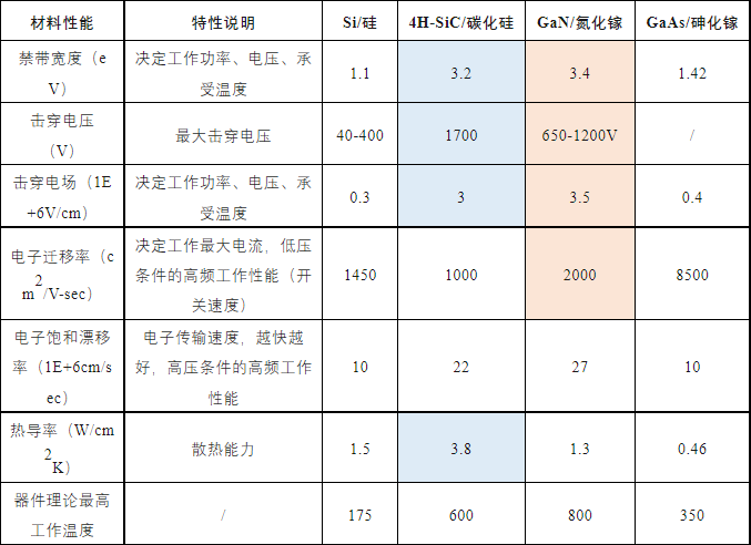
Comparison of Semiconductor Material Characteristics
Bandgap Width: Silicon has a bandgap width of 1.1 eV, which is almost three times smaller than that of gallium nitride and silicon carbide. Therefore, gallium nitride and silicon carbide can easily support circuits operating at higher voltages, while they can not support circuits at lower voltages like silicon.
Breakdown Electric Field: The breakdown electric field of gallium nitride and silicon carbide is more than 10 times higher than that of silicon. This high breakdown field allows gallium nitride and silicon carbide to handle higher voltages with ease.
Electron Mobility: The electron mobility of gallium nitride is three times higher than that of silicon carbide, making gallium nitride HEMTs more suitable for high-frequency applications.
Thermal Conductivity: The thermal conductivity of gallium nitride is 1.3 W/cmK (watts per centimeter Kelvin), which is lower than that of silicon. However, silicon carbide has the highest thermal conductivity and is three times better at transferring heat load compared to gallium nitride and silicon. This superior thermal performance gives silicon carbide a significant advantage in high-power and high-temperature applications.
(二)Comparison of Substrate Materials for Ga HEMT
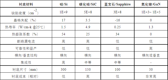
Comparison of GaN HEMT Parameters for Different Substrate Materials
Because GaN HEMT structures are epitaxial structures, different substrate materials can be used.
Attachment: Introduction to Device Structures
In order to facilitate a better understanding of the device structures mentioned in the text, a brief description of abbreviations for various types of device structures is provided.
MOSFET: Metal-Oxide-Semiconductor Field-Effect Transistor, abbreviated as MOSFET, is a voltage-controlled device. There are two types of MOSFETs, "p-channel" and "n-channel," and each type can be in either enhancement mode or depletion mode, resulting in four different types of MOSFETs.
BJT (Bipolar Junction Transistor): Bipolar junction transistor, commonly known as a transistor, is a current-driven device. There are two types of BJTs, PNP and NPN, which are widely used as amplifiers, oscillators, or switches, etc.
HEMT (High Electron Mobility Transistors): High electron mobility transistors.
pHEMT: Pseudomorphic High Electron Mobility Transistor, where "p" represents pseudomorphic.
IGBT (Insulated Gate Bipolar Transistor): Insulated gate bipolar transistor, which consists of MOS and PN as two basic units.
HBT (Heterojunction Bipolar Transistor): Heterojunction bipolar transistor.
Triacs: Triode for Alternating Currents, a bidirectional controlled silicon device.
Thyristor: Semiconductor controlled rectifier.
LDMOS (Lateral Diffused MOS): Lateral diffusion metal-oxide-semiconductor, a high-frequency high-power device. Initially, LDMOS was mainly oriented towards RF power amplifiers for mobile phone base stations.
CMOS (Complementary MOSFET): Complementary metal-oxide-semiconductor, composed of NMOS and PMOS, is the basic unit of integrated circuits.



Site Map | 萨科微 | 金航标 | Slkor | Kinghelm
RU | FR | DE | IT | ES | PT | JA | KO | AR | TR | TH | MS | VI | MG | FA | ZH-TW | HR | BG | SD| GD | SN | SM | PS | LB | KY | KU | HAW | CO | AM | UZ | TG | SU | ST | ML | KK | NY | ZU | YO | TE | TA | SO| PA| NE | MN | MI | LA | LO | KM | KN
| JW | IG | HMN | HA | EO | CEB | BS | BN | UR | HT | KA | EU | AZ | HY | YI |MK | IS | BE | CY | GA | SW | SV | AF | FA | TR | TH | MT | HU | GL | ET | NL | DA | CS | FI | EL | HI | NO | PL | RO | CA | TL | IW | LV | ID | LT | SR | SQ | SL | UK
Copyright ©2015-2025 Shenzhen Slkor Micro Semicon Co., Ltd