Service hotline
+86 0755-83044319
release time:2023-10-12Author source:SlkorBrowse:14849
Completing a semiconductor chip involves many steps, and it is important to screen out defective chips through testing. Many tests are conducted during the semiconductor manufacturing process.
- EDS (Electrical Die Sorting), also known as wafer test or probe test, is performed when the wafer processing is complete in the FAB step.
- The final test is performed after the chip is packaged.
Today we will learn about EDS, which is the first in a series of tests that ensure the quality of semiconductor chips.
EDS is related to improving the yield of semiconductors.
EDS occurs between the FAB step (where circuits are drawn onto wafers) and packaging step (where the chip has the appearance of the final product). As the name suggests, electrical testing is conducted on each chip to ensure it meets the required quality level. The purpose of EDS is as follows:
- Screen out defective semiconductor chips at the wafer level to improve subsequent packaging and testing steps, and save costs.
- Repair defective chips to improve yield and save costs.
- Correct problems found in design or FAB.
First, test the electrical characteristics to ensure that each chip meets the required quality level. Defective but repairable chips are repaired, and defective chips that cannot be repaired are marked with "ink". Defective chips are removed from subsequent processes to improve process efficiency.
EDS is crucial for improving semiconductor yield. The yield is the percentage of good dies that meet quality requirements relative to the maximum number of chips on a single wafer (GDPW, Gross die per wafer) and is a direct indicator of semiconductor production efficiency.
The EDS process is performed by making contact between the wafer and the probe card. Countless small pins on the probe card come into contact with the wafer and send electrical signals that can screen out defective chips.
There are four main steps in the EDS process, although many small processes make up EDS.
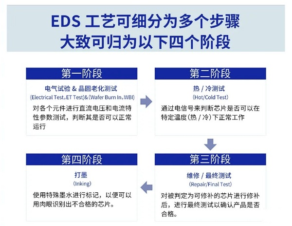
Step 1 - Electrical Test and Wafer Burn-In (ET and WBI)
Electrical test involves measuring the DC voltage and current characteristics of various components (transistors, resistors, capacitors, and diodes) required for the operation of semiconductor integrated circuits.
Following the electrical test is the wafer burn-in test. The wafer is heated to a certain temperature and then subjected to both AC and DC voltages to detect any defects or potential issues. This step greatly enhances the reliability of the product.
Step 2 - Hot/Cold Testing
In hot/cold testing, individual defective chips are detected on the wafer using electrical signals. Repairable defective chips are marked for repair in the subsequent step. To ensure the chips operate perfectly at different temperatures, they are tested at temperatures higher and lower than room temperature.
Step 3 - Repair/Final Testing
The repair step is perhaps the most crucial step in the EDS process.
In the repair step, chips that were deemed repairable in the hot/cold testing step are repaired. After repair, a final testing is conducted to validate that the repair has been performed correctly. The pass/fail result from this step is the final outcome.
Step 4 - Ink Marking
In the ink marking step, defective chips are marked with special ink to identify them. Chips that undergo ink marking include those that failed the hot/cold testing, were improperly repaired and failed the final testing, or were not properly completed on the wafer (dummy dies). In the past, actual ink marks were used to label the defective chips, but nowadays, only data is recorded to identify the defective ones. Defective chips identified through ink marking are not processed further in packaging, saving materials, equipment, time, and labor in the packaging and testing processes.
After ink marking, the wafer is baked, undergoes quality control (QC) inspection, and then proceeds to the packaging process.
We are now just a few steps away from the birth of a flawless semiconductor chip. In the next article, we will explore the packaging process of semiconductor chips into a form suitable for installation in devices.



Site Map | 萨科微 | 金航标 | Slkor | Kinghelm
RU | FR | DE | IT | ES | PT | JA | KO | AR | TR | TH | MS | VI | MG | FA | ZH-TW | HR | BG | SD| GD | SN | SM | PS | LB | KY | KU | HAW | CO | AM | UZ | TG | SU | ST | ML | KK | NY | ZU | YO | TE | TA | SO| PA| NE | MN | MI | LA | LO | KM | KN
| JW | IG | HMN | HA | EO | CEB | BS | BN | UR | HT | KA | EU | AZ | HY | YI |MK | IS | BE | CY | GA | SW | SV | AF | FA | TR | TH | MT | HU | GL | ET | NL | DA | CS | FI | EL | HI | NO | PL | RO | CA | TL | IW | LV | ID | LT | SR | SQ | SL | UK
Copyright ©2015-2025 Shenzhen Slkor Micro Semicon Co., Ltd